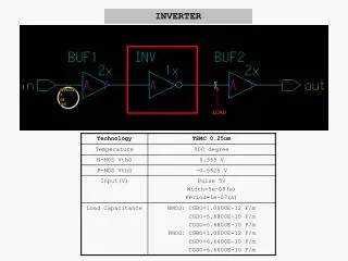

INVERTER
E N D
Presentation Transcript
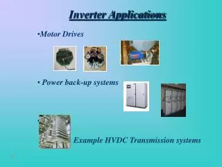
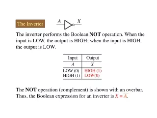
4.1 INTRODUCTION The category of converters, which converts dc power into ac power popularly known as the inverters. The application areas for the invertors includes the Uninterrupted Power Supply the ac motor speed controllers,etc. • The inverters can be classified based on number of factors like: • the nature of output waveform (sine, square, quasi square, PWM etc), • the power devices being used (thyristor, transistor, MOSFETs, IGBTs), • the configuration being used (series, parallel, half bridge, full bridge).
The size and the cost of the circuit can be reduced to some extent if the • operating frequency is increased but then the inverter grade thyristors • whichare special thyristors manufactured to operate at a higher • frequency must beused, which are costly. 4.2Basic Series Inverters (SelfCommutated Inverter) • The series inverter uses a class A type commutation. Thecommutatingcomponents L1, C1 are connected in series to form anunder damped tuned circuit. • Since the SCRs turn off themselves this circuit is known as commutated inverters .
Fig. (a )Basic series configuration Operation : • At instant t0 SCR1 is turned on. Let the initial voltage capacitor be“vc” withits left plate negative w .r. t. right plate and the sinusoidalload currentstarts flowing.
Fig (b) Mode 1 (t0 to t1) • The capacitor C1 start charging in the opposite direction as shown in fig B.The load current eventually comes to zero at instant t1 and SCR1 comes out of conduction due to natural commutation. • The voltage on the capacitor C1 at instant t1 is greater than V with its leftplate positive w.r.t. its right plate. • As there is no discharge path for the capacitor, this voltage will be heldconstant up to instant t2 where SCR2 is triggered.
Fig ( c ) Mode 2 (t1 to t2) • At instant t2, SCR2 is turned on and the load voltage and current both becomes negative. • The capacitor now discharges resonantly through SCR2, R, L1, as shown infig (c) • At instant t3 the discharge current goes to zero and SCR2 turned off again due to natural commutation. The voltage on C1 is equal to vc. • Off time :During the time interval between t1 and t2 both the SCRs are in the off state. Load voltage as well as load current are zero. Therefore this interval is known as off time of the circuit.
Disadvantages: • Limitation on the maximum operating frequency • Distortion in the output wave form • High rating of commutating components • The peak amplitude and duration of output current depends on the load parameters resulting in poor regulation for the inverter. • The power flow from the dc source is intermittent. Therefore, the dc supply must have a large peak current rating and the input current contains high percentage of harmonics.
Modified Series Inverter The operation can be divided into two modes. Mode 1: At the instant when SCR T2 is triggered, the voltage across the capacitor will be slightly less than (E c + E dc)and the load voltage and current will be closed to zero. Hence the voltage across the capacitor minus the load voltage will appear across L2.Since L1 is closely coupled to L2, the same voltage will appear across L1. Mode 2: The voltage across L1 will tend to increase the cathode potential of SCR T1 more than its anode potential and therefore, SCR T1 will be reverse biased and turn-off. Thus, even if SCR T2 is turned on before SCR T1 is switched off, it will not result into short circuiting of the d.c. source. A similar operation will take place if SCR T1 is triggered before SCR T2 is turned off.
Modified Series Inverter (Final) Note: L1 = L2 C1 = C2
Basic Parallel Inverter • A parallel inverter is used to produce a square-wave from a d.c. supply. • In this inverter, the commutating capacitor comes in parallel with the load during the operation of the inverter. Hence it is called as ‘parallel inverter’. Operation Mode 1: • This mode begins when T1 is fired and current flows through the inductance L and the thyristor T1. • When SCR is turned on, a d.c. voltage E dcappears across half the transformer primary, which means the total primary voltage is 2 E dc, hence the capacitor is charged to 2 E dc.
Mode 2: • This mode begins when thyristor T2 is fired. When T2 is turned on, the commutating capacitor applies voltage -2 Edc to appear across T1, it will be turn off. • SCR T2 will now be conducting and the voltage of 2 E dc will appear across the transformer primary and commutating capacitor, but with reverse polarity. • Mode 3: • During mode 3, this SCR is again turned on. Commutating capacitor applies a voltage -2 E dcto appear across T2. • when this reverse voltage is applied for sufficient time across T2, it will be turned off. If trigger pulses are applied periodically to alternate thyristors, an approximately rectangular voltage waveform will be obtained at transformer output terminals.
Parallel Inverter With Feedback Diodes The circuit operation can be divided into different operating modes. • Thyristor T1 and T2 are the main load carrying thyristors. • Inductor L and capacitor C are the commutating components. Diodes D1 and D2 are the feedback diodes. Which permit the load reactive power to be fed back to the d.c. supply.
Mode 1 :- • During this mode, thyristor T1 is triggered at instant R. • Battery voltage forces the current to the primary • section through path Edc -C-A-T1-L- E dc . Terminal C is • positive with respect to A. • The flux produced due to this current induces the • voltage in all sections of transformer winding. The • load voltage is nearly equal to Ede and is in such • direction so as to force current into the dot at • terminal P. Due to autotransformer action, voltage • Edc is induced in CE section of primary winding.
Mode 2: • This mode begins with thyristor T2 switched on at instant S. When T2 is turned on, capacitor C will immediately apply a reverse voltage of 2 E dcacross SCR T1 and turned off. When SCR T1 is turned off, the capacitor will discharge through SCR T2, inductor L, diode D1, and a portion of a transformer primary winding BA. • Thus, the energy stored in the capacitor will be fed back to the load through the transformer coupling of windings BA and PQ. • The load current which earlier flowing through SCR T1, will now flow through CB and diode D1 to negative input terminal. This can happen only if diode D1 is forward biased and capacitor discharge current is more than the load current.
The current through inductance L will now flow through diode D2, DE and SCR T2, and the trapped energy in inductor L will be fed back to the load. D point is now connected to the negative supply terminal, the load voltage polarity will be reversed. • Also capacitor C will be charged in the opposite direction slightly more than supply voltage. Thyristor T2 will stop conducting. Energy is transferred from the capacitor and inductor to the load. • Mode 3 : • This mode begins with when load current becomes zero, diode D2 will be blocked and SCR T2 will have to triggered again at instant U to reverse the direction of the load current. When thyristor T2 starts conducting, the load voltage will again become equal to Edc.
Single Full Bridge Inverter A serious drawback of the half bridge inverter is that, it requires a 3-wire dc supply. This is overcomedby the commonly full bridge inverter. Introduction –
Construction: • It has consist of four thyristor and four • freewheeling diode. • Two thyristor T1 and T2 must be gated • simultaneously at frequency F=1/T and thyristor T3and T4 must be gated 180 out of phase frequency can be controlled by varying the periodic time T.
Operation- • When we apply positive load voltage Edc then thyristor T1 and T2 conduct. • When we apply negative voltage –edc then thyristor T3and T4 is conduct. • Diode D1to D4 serve to feed the load reactive power back to the dc supply. • In place of SCRT1, hear two thyristor T1 and T2 conduct similarly in place of SCR2 thyristor T3 and T4 conduct and in place of D1 and diodeD1, D2 conduct, where as instead of D2, hear D3and D4 conduct • The load voltage wave form is fairly rectangular and is not affected by the nature of the load.
Advantage : • No need of an output transformer. • Efficiency is high. • The current rating of power device is equal • to the load current. • Disadvantage : • Number of four transistors are required • Costs is high • Application : • Used in commutation circuit for bridge • inverter
Construction :- • It is a complementary impulse commutated inverter. • This means that if two inductors are tightly coupled, triggering of one thyristor , turnsoff another thyristor . • Main thyristors T1,T2 . • Feedback diodes D1,D2. • two capacitors C1,C2 . • magnetically coupled inductors L1 and L2. • inductance L .
Operation Mode- 1 • Thyristor t1 is triggered, then SCR T1 is turn on, upper d.c. source load current Il to the load. • As the load current is constant. Voltage drop across L1 is negligible. With zero voltage drop across L1 , T1 , C1 and across C2 is Edc load. Mode -2 • When SCR T2 is triggered ,turn off the SCR T1 • voltage across C1 and C2 cannot be change • equal voltages is induced across L1 • Voltage across thyristor T1 is ET1 = Edc • Ic1 = Ic2 KCL at node ‘o’ in fig. Ic1 + Ic2 = Il + Il ; IC1 = IC2 =Ic3
Mode -3 • At instant t1 , where capacitor C1 is charged to supply voltage Edc , i.e. Ic 1 =0 at t 1, Vc 2=0. Just after t 1, current ( Il + Im/2) through C1 tends to charge it with bottom plate . • At t1 ,the energy stored in inductor L2 is dissipated. • This energy is dissipated at instant t 2, therefore I2 decays to zero & a result SCR T2 is turned off at T2. Mode -4 • When the current IT2 through L2 & T2 has decayed to zero . the load current IL=ID2 still continues flowing through the diode D2 as ID2 during (t3-t2 ) interval.
Mode -5 • As soon as iL equal to ID2.tend to reverse , diode D2 is blocked. • Thyristor T2 already gated during the interval (t3-t2)gets turn ON to carry the load current in the reverse direction . • The capacitor C1 , now charged to the source voltage Edc is ready for commutating the main thyristor T2 .
Operation :- • Mc Murray Bedford full bridge inverter circuit can be realized by connecting two half bridge inverters. • for Mode 1, thyristors T1 and T2 are conducting and load current flows through Edc, T1, L1 load Zl , L2, and T2. • Voltage across C1, C2 is zero but capacitors C3, C4 are charged to voltage Edc. • For initiating communication of T1, T2 thyristors T3, T4 are triggered. • This reverse-biases T1, T2 by voltage (-Edc) and makes them turned-off.
4.3 PULSE –WIDTH MODULATION • Pulse-width modulation technique is a control within the inverter & is also known as a variable-duty-cycle regulation. • This method of regulation employs variation of the conduction time per cycle to alter the rms output voltage of the inverter. In order to accomplish this regulation technique.
0peration:- • In fig, SCR1&SCR2 - Two main loads carrying SCRs SCR3, SCR4 - Two auxiliary SCRs which are of smaller rating C1 & C2 - Two separate commutating capacitors. • When, SCR1 - ON • Power is delivered to the load at the same time, C1 is • charged to the voltage ofthe transformer section AB • with a polarity as shown above fig, SCR1 -OFF
At any desired instant by triggering SCR3 • After interval, SCR2 – ON • To deliver power in the negative half-cycle. • C2 charged at the same time by the voltage of transformation • section CD. • SCR2 - OFF by firing SCR4 • In this method produces a quasi-square-wave output • as below in fig,
Single pulse width modulationThere is one pulse per half-cycle, and its width is varied
The modulation index is: • The rms output voltage is: • Advantages: • Less effect of noise • synchronization between the transmitter & receiver is not essential. .
Disadvantages: • In order to avoid any wave form distortion, the • bandwidth required for the PWM communications large as • compare to BW of PAM • Average power transmitted can be as low as 50% of • maximum power • Application: • voltage regulators. • class D audio amplifiers ,which are highly effectively. • The following fig, shows the harmonic reduction profile with • variation of the modulation index M
The domain harmonic is the third and DF decreases significantly • at alow output voltage.
Multiple pulse modulation • The harmonic contents can be reduced by using several pulses in • eachhalf cycle of output voltage. This type of modulation is also • known asuniform-pulse – width-modulation • The number of pulses per half cycle is: Here, = modulation frequency ratio mf • The rms output voltage is:
The following waveform shows the harmonic reduction against • variation of the modulation index & P=5
Sinusoidal pulse modulation • Instead of maintaining the width of all pulses the same, the width • of each pulse is varied in proportion to amplitude of a sine wave • This kind of modulation is known as SPWM. • The rms output voltage is: