Download

1 / 38
380 likes | 712 Vues
A Novel Method for the Fabrication of High-Aspect Ratio C-MEMS Structures. Outline. Objective Introduction Experimental Results and Discussion C-MEMS structures with Overhangs Importance of Baking Source Self Organization of Resist features in 2-D Arrays 3-D Suspended C- MEMS

E N D
A Novel Method for the Fabrication of High-Aspect Ratio C-MEMS Structures
Outline • Objective • Introduction • Experimental • Results and Discussion • C-MEMS structures with Overhangs • Importance of Baking Source • Self Organization of Resist features in 2-D Arrays • 3-D Suspended C- MEMS • Conclusion
Objective • To give idea about MEMS fabrication techniques and detail about one recent work in the field, which could make greater impacts in the micro fabrication , that is about a Novel method for the Fabrication of High aspect ratio C-MEMS Structures
“There is Plenty of Room at the Bottom” • Proffesor Richard P. Feynman gave his famous lecture titled “There is Plenty of room at the bottom” on December 26, 1959, at the annual meeting of the American Physical society at the California Institute of Technology.
“There is Plenty of Room at the Bottom” • In it he described the enormous amount of space available on the micro scale, ‘The entire encyclopedia could be written on the head of a Pin’
Introduction MEMS • It refers to devices have a characteristic length of less than 1mm but more than 1 mm, that combine electrical & Mechanical Components • Originated as a result of advances in Microelectronics and Invention of Transistors in 1948 • Invention of Integrated Circuit in 1959 by Kilby boosted the Micro Fabrication techniques
Manufacturing Techniques For MEMS • Surface Micro Machining • Bulk silicon Micro Machining • Lithography • Lithography,Electro deposition(plating) and plastic Molding (or its German, Lithographie, Galvanoformung, Abformung [LIGA]) • Electro Discharge Machining
MEMS-Silicon and Carbon • Conventional MEMS is mostly based on silicon • Recently , microfabrication of Carboneous material has received a lot of attention. • The different Crystalline structures and Morphologies enable Carbon, different physical, chemical, thermal and electrical uses. • Micro fabrication of Carboneous Materials are called C- MEMS
MEMS fabrication for Carbon Structures • Current processing Technology for the Microfabrication of Carbon structures are -Focused Ion Beam -Reactive Ion etching • They have the following disadvantages -Time Consuming -Expensive
Photoresists • Photoresist -The photoresistive compound used in microfabrication is called Photoresist or simply resist • Positive Photresist -It responds to light in such a way as to make the exposed regions dissolve more quickly during the development process. • Negative Photoresist -It responds in the opposite manner. Unexposed regions of the resist will dissolve in the developer While exposed regions remain behind
In this work -Photoresist derived C-MEMS structures were obtained in a two step pyrolysis process in an open ended quartz-tube furnace • First -The samples were baked in a N2 atmosphere at 3000C for about 40 min first • Second -heated in a N2 atmosphere upto 9000C, at this point the N2 gas is shut off and forming gas [H2 (5%)/ N2 ] is introduced for one hour • Then -the heater is turned off and the sample is cooled down again in N2 atmosphere to room temperature [cooling time 10hr(100C/min)]
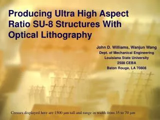
C-MEMS Structures with Overhangs • We have seen that how SU-8 Photoresist is used to create High- Aspect ratio posts with high resolution and Pattern fidelity • In this work, Marc.J.Madau et al developed novel techniques to form complicated Suspended C-MEMS by nontraditional process recipes such as over exposure, underdevelopment, directed flow of the developer and exploitation of surface tension in the developing Photoresist pattern
Importance of Baking Source • With Some imposed baking parameters a hard top layer can easily be observed • In an Oven the resist is uniformly heated by convection from all sides. • Skin formation on the resist surface is often observed, which reduces further solvent evporation. • In general oven-baking for straights SU-8 posts tend to lead to T-Shaped hats whereas a hot plate keeps the original shoe more in-tact. • Oven baking also creates a hard skin on unexposed resist thereby forcing the developer to attack the unexposed resist parts faster from the sides than from top leading to overhangs and Tunnels
SEM photos of 3-D suspended structures. (a) and (b): before pyrolysis; (c) and (d): after pyrolysis.
Self Organisation of the resist features • Self organized groups of Carbon posts- a feature most readily observed for high aspect ratio C- MEMS arrays with posts higher than 300mm • The figure shown in (a) demonstrate that posts aggregation occurred before pyrolysis • When the Post bake temperature is above the transition temperature, the unexposed area reflows and this could enable the posts to move forward each other • There is agregation/bunching happened, the mask patterns are transferred with high fidelity
SEM photos of self organized patterns: (a) SU-8 structure before pyrolysis: (b), (c), and (d) Carbon structure after pyrolysis.
Collapse of Carbon Posts • Using too high a pressure on the Nitrogen drying gun the developed high aspect ratio post patterns randomly collapsed as shown in fig (a) Inset. • The effect caused by the large internal stress can be alleviated either by reducing the total exposed arc or by generating discrete small-sized exposed regions.
Remedy • We can Overcome stress problems and successfully turn the photoresist structures into C-MEMS without cracks, if we use the above described two step pyrolysis process • When the developer solution is removed gently this pulls posts that are tall and close enough together into symmetric patterns • The rules controlling the Number of posts per bunch has not yet been investigated and further experiments are needed to understand how the different types of symmetric bunches organize themselves
3-D Suspended C-MEMS • We have seen that self Organized bunched C-MEMS posts can be made. • Now, by introducing non traditional lithography process steps, such as underdevelopment, doping of the photoresist with Nanoparticles, we can controll the developing flow direction • By Using SU-8 Photoresist doped with Fe2O3 nanoparticles, it is found that the formation of suspended Structures can be controlled much better • By proper control of the soft bake, exposure, and development time, suspended carbon fibers can also be built as shown • Investigations are going to make thinner suspended carbon wires
SEM photos of suspended carbon fibers by using modified SU-8 photoresist. (a) SU-8 before pyrolysis; (b), (c), and (d): C-MEMS after pyrolysis.
Complex C-MEMS Structures • By careful control of the geometrical distribution of the posts in the array and the over exposure dose, a wide variety of suspended and complex C-MEMS Structures, such as plates and bridges(as shown in next figure) , can be fabricated
SEM photos of suspended C-MEMS structures formed from modified SU-8 100.
Improvement of fabrication • In order to improve patterning quality and shorten the processing time both immersion and spray development was used to develop thick and dense SU-8 arrays • By actively controlling the spray direction of developer to attack the exposed resist from one direction only, we can further control the resulting patterns to build, for example, ribbon like SU-8 Structures. Carbon ribbons after pyrolysis is shown in the figure
C-MEMS microbattery • The processes described earlier can easily be extended to two layers or multi layer C-MEMS structures • In the figure shown in the next slide, in the C-MEMS battery, the current collector for rows of anode and cathode posts in the second layer of the carbon
Conclusion • The C-MEMS pyrolysis of thick photoresist provides a powerful new carbon microfabricatin technique, which has potential application in Carbon based electronics, sensors, batteries, microfluidics etc. • Although there is shrinkage in both height and width, the C-MEMS structures mostly retain the original SU-8 photoresist shape • By careful control of processing parameters and heating conditions, a variety of complex 3-D MEMS structures, such as suspended carbon wires, bridges, plates, self organized bunched posts(Carbon Flowers) and networks were built
The photoresist derived high aspect ratio C -MEMS arrays can be charged and discharged with Li ions providing a promising material for microfabrication solution to current battery miniaturization problem. • As the manufacturing techniues for MEMS are in the initial stages, a detailed analysis and testing are not possible. Observation and rule of thumb still persists. So the scope of engineers to involve in this work is high
References • Chunlei Wang,Guangyao Jia, Lili H. Taherabadi, and Marc J. Madou “A Novel Method for the Fabrication of High-Aspect Ratio C-MEMS Structures” JOURNAL OF MICROELECTROMECHANICAL SYSTEMS, VOL. 14, NO. 2, APRIL 2005 pp.347-357. • Chunlei Wang,Guangyao Jia, Lili H. Taherabadi, Marc J. Madou, Yuting Yeh and Brauce Dunn” C- MEMS structures for the manufacturing of 3-D Microbatteries”. Electrochemical and solid state letters. October 19, 2004 pp A435-A438 • W.H. The, U-Dwing, G-Salis, R. harbers, U Dreshler and R.F Malort, C.G.Smith, H.J .Guntherodt.”SU-8 for real three dimensional and sub diffraction-limit two photon microfabrication” Applied Physics letters, Vol 84 November 20, 17 May 2004. • Marc J Madou, “MEMS Fabrication” The MEMS hand book, CRC Press pp 16-1 to 16-165.
Stephen a campBell, “ The Science and electronics of Microelectronic fabrication” Oxford Publications pp 182-199. • F.G.Tseng, Y. J Chaung, and W.K Lin.”A novel; fabrication method of embedded microchannels employing simple U.V dosage control and anti reflection coating” papers from MEMS 2002 ieee international conference at Las Vegas, pp 70-72. • Mohamed Gad-el Hak ”Introduction to MEMS”. The MEMS Hand Book, CRC Press, pp 1-1 to 1-5.