Download
1 / 20
250 likes | 508 Vues
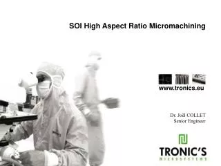
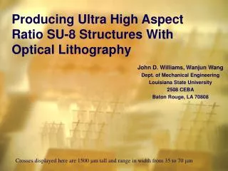
Producing Ultra High Aspect Ratio SU-8 Structures With Optical Lithography. John D. Williams, Wanjun Wang Dept. of Mechanical Engineering Louisiana State University 2508 CEBA Baton Rouge, LA 70808. Crosses displayed here are 1500 m tall and range in width from 35 to 70 m.

E N D
Producing Ultra High Aspect Ratio SU-8 Structures With Optical Lithography John D. Williams, Wanjun Wang Dept. of Mechanical Engineering Louisiana State University 2508 CEBA Baton Rouge, LA 70808 Crosses displayed here are 1500 m tall and range in width from 35 to 70 m
High Aspect Ratio Microfabrication • The production of mechanical systems often requires 3 dimensionality in the design. • To achieve 3-D structures, designers often transfer complex 2-D patterns deep into a substrate. • Currently there are three transfer procedures that yield significant height to width aspect ratios. • Deep x-ray lithography (aspect ratios >150:1). • Deep silicon etching ( >75:1). • SU-8 UV lithography ( >15:1).
Advantages of High Aspect Ratio Processes • Provides engineers with the ability to produce tall mechanical structures. • Allows for the development of fluidic vias and very narrow diffusers. • Provides the ability to achieve “3-D” structures on the micro scale.
UV Lithography With SU-8 • Optimized for producing MEMS devices. • Spun to thickness' between 10 and 1500 m . • Demonstrated aspect ratios of 25:1 using UV-lithography. • Best performer to date for thick resist processing with ultraviolet light. • Can be patterned using a common broadband contact aligner.
Advantages of SU-8 Processing for High Aspect Ratio MEMS • Lithography does not require and expensive light source. • SU-8 processing can be done using common cleanroom equipment. • 3-D structures can be fabricated easily using multiple exposed layers. • Mature electroplating processes developed for LIGA processing allow for a wide choice in material selection.
Disadvantages of SU-8 Processing • Extremely difficult to define proper bake parameters. • Resist remains “soft” until after exposure. • High concentrations of stress in resist are present during traditional processing. • Solid polymer is highly self adhesive. • Exposed SU-8 is extremely difficult to selectively remove.
Current SU-8 Process Technology • Patterns are currently transferred 1500 m into resist with aspect ratios of 5:1. • 25:1 aspect ratios are commonly presented in structures between 100 and 400 m tall. • Recent work demonstrates the ability to achieve 15:1 trenches in 100 m of resist and 50:1 featured patterns in 600 m of resist.
Visual Picture of the State of the Art in SU-8 UV Lithography • Dentinger et.al., Microelectronics Engineering.61-62 (2002)1001-1007. • Lin et.al., J. Micromech. Microeng. 12 (2002) 590-597. • Loechel., J. Micromech. Microeng.10 (2000)108-115.
Methodologies for Improving the Aspect Ratio of SU-8 Processes • Chemical modification of the resist. • Addition of high refractive index material between resist and mask to reduce diffraction. • Use of selective UV spectrum. • Reduces effects of diffraction. • Eliminates short wavelengths that are absorbed in the first few microns of the resist leading to pattern distortion.
Results Achieved Using Process Improvements • Wavelength filtering • Ling et.al., Proc. of SPIE. 3999 (2000) 1019-1027. • Chemical Modification • Ruhmann et.al., Proc. of SPIE. 4345 (2001) 502-510. • Before and after diffraction reduction w/ 365 nm light • Chuang, Tseng, lin. Microsys. Tech.8 (2002) 308-313.
Our SU-8 Process • SU-8 resist without any modifications • No specific filtering • No diffusive control by added materials between mask and wafer • Optimized spin and bake procedures • Optimized exposure conditions • Room temperature development in stagnant fluid
Issues Present in Process • How to coat SU-8 in layers greater than 800 m successful? • Multiple coats for layers over 1100 m. • Maintaining a level surface until after exposure is critical. • What are the proper bake conditions for very thick resist layers? • Approximately 50min/100 m of resist at 96 C in an oven. • Films greater than 1mm require slightly elevated temperature if hotplate is used. • Multiple coatings require extra bake time. • Stress reduction obtained by proper cooling of sample. • What is the optimal exposure dose required to achieve the pattern? • Open field structures require significantly more dose than holes and closed structures.
Experimental Results • We have greatly reduced the internal stress in SU-8 films. • We have developed a repeatable procedure for achieving 1500 m thick layers. • Have established optimal exposure doses for films 1000, 1200, and 1500 m thick. • Demonstrate the ability to produce open field structures, including cylinders, with high aspect ratios. • Demonstrate the ability to pattern holes in closed structures as deep as 1200 m.
High Aspect Ratio Features Produced in This Experiment • 35 and 50 m wide crosses 1500 m tall.
1150 m Tall Cylinders With Varying ID and Wall Thickness’ • Inner diameters vary from 40 m to 200 m. • Optical image shows complete development of the cylinders. • Cylinder with wall thickness’ less than 30 m collapsed.
1150 m Tall Cylinders With Min. Wall Thickness of 50 m • Aspect ratio > 23:1. • Optical image in corner shows that the resist was completely developed away inside the cylinders.
1150 m Tall Crosses 25 m Wide • Aspect ratio 46:1. • Open field, free standing structures require higher doses than cylinders or hole patterns.
How High of an Aspect Ratio Can Be Achieved? • 50:1 is easily obtainable. • Here one can see a 100:1 pattern (6 m wide and 630 m tall). • A 7 m trench is also observed from top to bottom of the features. • Required new development process. • 630 um tall patterns. Numbers • represent the width of the • feature on the mask pattern.
Concluding Remarks • We are able to obtain high aspect ratios using a simple SU-8 lithography process that can be applied in almost any MEMS laboratory. • We demonstrate, for the first time, the ability to achieve 100:1 aspect ratios that cannot be produced using any lithographic technique other than x-ray lithography. • We believe that the exposure can be improved simply by using repeatedly published process modifications.
Acknowledgements • National Science Foundation • NSF Grant ECS-#0104327 • Louisiana Space Consortium (LaSPACE), NASA • Center for Advanced Microstructures and Devices (CAMD) at Louisiana State University