Download
1 / 18
270 likes | 860 Vues
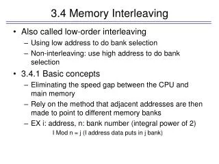
3.4 Memory Interleaving. Also called low-order interleaving Using low address to do bank selection Non-interleaving: use high address to do bank selection 3.4.1 Basic concepts Eliminating the speed gap between the CPU and main memory

E N D
3.4 Memory Interleaving • Also called low-order interleaving • Using low address to do bank selection • Non-interleaving: use high address to do bank selection • 3.4.1 Basic concepts • Eliminating the speed gap between the CPU and main memory • Rely on the method that adjacent addresses are then made to point to different memory banks • EX i: address, n: bank number (integral power of 2) I Mod n = j (I address data puts in j bank)
Consecutive accesses to contiguous locations will be routed to different (interleaved) memory banks • Overlaps the two bank’s activities and increase the CPU-memory bus bandwidth • The overlapping means that while one-memory bank is busy accessing its data to respond to the processor’s request, the other bank is free to receive the next request. • DRAM: cycle time = Ta (access time) + Tpr (precharge time) • Interleaving is used to overlap the access time of one memory bank with the precharge time of another memory bank
32-bit non-interleaved 4bytes/100ns = 40 Mbytes/sec
2-way doubleword -interleaved 4bytes/50ns = 80 Mbytes/sec
EX 3.12: using the DRAM controller in a 2-way word-interleaved memory • CPU has 16-bit data bus with a bus cycle time 50ns design a 1-Mbyte DRAM memory • Due to two-way interleaved, we can use 100 ns DRAM to provide 50 ns bus cycle time • Bank 0: 2N, 2N+1, Bank1: 2N+2, 2N+3 • 1Mbyte requires A0-A19 address line • A0: section select • A1: bank select • A2-A19: word address line
Fig. 3.28: CPU with 32-bit data bus, to form 2Mbyte with 2-way • 2 Mbyte: A0 –A20 A0, A1: section select, A2: bank select, A3-A20 double-word address line, each bank require 256Kbit*8*4
Four-way double-word interleaving • Motorola 680x0 CPU with address line A0-A31, 32 data bus. Use 64K*8-bit memory chip to form a 2 Mbyte four-way interleaving memory in high physical address space • 2Mbyte = 64Kbyte*32 (A0-A20 is used to address space, A21-A31 is all one • 32/4-way = 8 chip (i.e., each bank has 8*64 Kbyte) • 32-bit data bus32/8=4 section each bank each section has 2*64Kbyte (2 rows) • A0, A1: section selection • A2, A3 : bank selection • 64 KA4-A19 is address line • A20 is row selection ( every 64 kbyte change to another row) or A4 is row selection (every 16 bytes change to another row), A5-A20 is address line • A21-A31 is all 1 • Big-endian: section 0 connect to D31-D24
3.5 Memory time computation • Tc: the memory cycle time • Tadress-cycle: the CPU address-cycle • For introducing no wait states in the processor cycle, we need N-way interleaving, where N = Tc/ Tadress-cycle • EX: Intel i86 CPU with 32-Mhz clock, the main memory is 125-ns DRAM • C=1/32MHz = 31.25 ns, • Bus cycle = 2 clock cycle Taddress-cycle =62.5ns • Ta = 125 ns tc = 250 ns N = 250/62.5 = 4 • 4-way interleaving will not introduce wait state