Download
1 / 1
30 likes | 176 Vues
This paper discusses an innovative method of application-specific memory interleaving designed to enhance performance in FPGA-based grid computations. It addresses challenges in molecular dynamics, physics, and image processing, highlighting the need for custom memory access patterns due to irregular data access orders. The approach leverages FPGA's capabilities for fine-grained parallelism, providing optimized algorithms that differ significantly from traditional sequential methods. The framework aims to unlock extensive computational potential while addressing memory access constraints through custom interleaving structures.

E N D
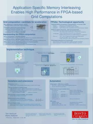
1 0 3 2 1 0 0 1 2 3 0 1 BOSTON UNIVERSITY www.bu.edu/caadlab Application-Specific Memory Interleaving Enables High Performance in FPGA-based Grid Computations Grid computation: candidate for acceleration Many applications in molecular dynamics, physics, molecule docking, Perlin noise, image processing … Computation characteristics being addressed: Cluster of grid points needed at each step Grid cells accessed in irregular order Invalidates typical schemes for reusing data Working set fits into FPGA’s on-chip RAM Implementing for FPGA computation Allows reconsideration of the whole algorithm Optimal FPGA algorithms are commonly very different from sequential implementations Developer has access to algorithm’s logical indexing scheme Extra design information in 2,3,... dimensional indexing, before flattening into RAM addresses FPGAs support massive, fine-grained parallelism in computation pipeline Often throttled by serial access to RAM operands Goal: Fetch enough operands to fill the width of the computation array FPGAs: Technological opportunity Traditional memory interleaving for broad parallelism – in use since 1960s Generic: Designed to avoid application specifics Fixed bus: All applications use same memory interface Expensive: High hardware costs, accessible only for major processor designs FPGAs for memory interleaving – ideal technological match Customizable: Can adapt to arbitrary application characteristics Not just permitted, customization is inherent and compulsory Configurable: Unique interleaving structure for each application Multiple different structures for different parts of one application Free (almost) : 10s to 100s of independently addressable RAM busses On-chip bus widths 100s to 1000s of bits Cheap, fast logic for address generation & de-interleaving networks FPGA-based computation is an emerging field Does not have software’s huge base of widely applicable techniques Needs to develop a “cookbook” of reusable computation structures Bilinear interpolation for computing off-grid points Implementation technique 2. Round up to power of 2 bounding box RAM banks indexed by {X, Y} mod 4 4. De-interleaving: Map RAM banks to outputs 3b 3d 3a 3c 2b 2d 1 2a 2c 1b 1d 1a 1c 0 1. Define application’s access cluster Convert to rectangular array 0 1 3. Address generation: Map access cluster to grid Handle wraparound: {X, Y} / 4 vs {X, Y} / 4 + 1 The general case, not just limited to 1D or 2D arrays MSBs X +1? Address generation Y +1? 3a 3b 3c 1 2a 2b 2c RAM array 0 1 2 3 1b 0 De-interleave LSBs A B C D 0 1 Variations and extensions Dimensions: 1, 2, 3, … Adapts easily to dimensionality. Adapts easily to cluster size & shape. Can use non-power-of-2 memory arrays LSBs become X mod NX – efficient implementations for modest NX MSBs become X div NX – efficient implementations using block multipliers Allows wide range of design tradeoffs: Logic & multipliers vs. RAMs Latency vs. hardware Take advantage of dual-ported RAMs, when available Allocate less hardware to small grids Optimize de-interleaving multiplexers 4x4x4 RAM array requires 64:1 output multiplexers Implement efficiently as three layers of 4:1 multiplexers Write port design choices Can use dual-ported RAM for non-interfering, concurrent read & write Write single words or clusters – need not be same shape as read cluster Automation Java program – initial version available Seehttp://www.bu.edu/caadlab/publications Source code and documentation Sample input for hex grid example above name=HexGrid Name of VHDL component axis=horiz axis=vert Symbol names for axis indices databits=16 Width of individual word output=B1,0,1 output=A2,1,0 Define the access cluster output=B2,1,1 output=C2,1,2 output=A3,2,0 output=B3,2,1 output=C3,2,2 testSize=150,75 Grid size for test bench VHDL output HexGrid.vhdlSynthesizable entity definition HexGrid_def.vhdlDeclaration package HexGrid_test_driver.vhdlTest bench - confirms implementation Y0:1 Z0:1 X0:1 Output Tom VanCourt Martin Herbordt {tvancour, herbordt} @ bu.edu • Barnes, George H., Richard M. Brown, Maso Kato, David J. Kuck, Daniel L. Slotnick, and Richard A. Stokes. The Illiac IV Computer. IEEE Transactions on Computers 17(8), August 1968 • Böhm, A.P.W., B. Draper, W. Najjar, J. Hammes, R. Rinker, M. Chawathe, and C. Ross. One-step Compilation of Image Processing Applications to FPGAs. Proc FCCM. 2001 • M. B. Gokhale and J. M. Stone. Automatic Allocation of Arrays to Memories in FPGA Processors With Multiple Memory Banks. Proc. FCCM 1999