Understanding Computer Architecture and Instruction Execution Cycle
This article explores the fundamental components of computer architecture, focusing on the fetch-execute cycle, instruction set design, and the role of the control unit. It outlines the steps required to execute assembly language instructions, including fetching, decoding, reading operands, and executing the instruction. Additionally, the classification of instructions into memory, register, and I/O operations is discussed, emphasizing how each is implemented in a typical architecture. The importance of efficient instruction sets and clock timing in executing operations is also highlighted.

Understanding Computer Architecture and Instruction Execution Cycle
E N D
Presentation Transcript
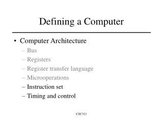
Defining a Computer • Computer Architecture • Bus • Registers • Register transfer language • Microoperations • Instruction set • Timing and control CSC321
Internal Operation • To execute an assembly language instruction the processor goes through 4 steps • Fetch an instruction from memory • Decode the instruction • Read the operands from memory/registers • Execute the instruction • This is often referred to as the Fetch-Execute cycle or the Instruction cycle • To execute a program the processor repeats this cycle until a halt instruction is reached CSC321
Bus Architecture S2 Access Select Memory unit 4096x16 111 S1 S0 address 001 AR 010 PC 011 16-bit Bus DR E ALU 100 AC INPR 101 IR 110 TR OUTR clock CSC321
Instructions • We said previously that there are two parts to an instruction • Opcode • Operand • Realistically the two parts should be called • Opcode • Everything else CSC321
Instructions • Three basic types • Those that reference memory operands • Those that reference register operands • Those that reference I/O devices • Again, this is only for the fictitious architecture in the textbook but you will find similar categorizations in real architectures CSC321
Instruction Decoding • The control unit evaluates bits 15 – 12 to determine the instruction format • At first glance it appears that there can be only 8 unique instructions since the opcode resides in 4 bits • But, additional instructions are created through the use of the I bit an unused bits in the operand field CSC321
Instruction Set Design • To be useful, an architecture’s instruction set must contain enough instructions to allow all possible computations • Four categories are necessary • Arithmetic, logical, shift operations • Moving data to/from memory from/to registers • Control such as branch and conditional checks • Input/output CSC321
Instruction Set Design • The set in the book is complete in that all the possible operations on binary numbers can be performed through combinations of instructions • But, the set is very inefficient in that highly used operations require multiple instructions • This is why the Pentium instruction set is so large and complicated – it makes for efficient programs CSC321
Memory Instructions • There are 14 instructions in this class • 7 direct memory address forms • 7 indirect memory address forms 15 14 12 11 0 I opcode address I = 0 means direct memory address I = 1 means indirect memory address CSC321
The “x”s represent the 12 bits of the operand field Memory Instructions CSC321
Register Instructions • There are 12 instructions in this class • They use the “operand field” to specify the register and type of operation since no memory address is required 15 14 12 11 0 0 1 1 1 Register operation CSC321
Operand field is “hard-coded” and specifies both the operation and operand (register) Register Instructions CSC321
I/O Instructions • There are 6 instructions in this class • They can use the “operand field” to specify the exact operation since no memory address is required 15 14 12 11 0 1 1 1 1 I/O operation CSC321
Operand field is “hard-coded” and specifies both the operation and operand (register) I/O Instructions CSC321
Lots of combination logic goes in here The Control Unit Instruction Register (IR) 15 14 - 12 11 - 0 Other Inputs 3x8 Decoder 12 Control Unit D7 – D0 n I T15 – T0 4x16 Decoder Increment Sequence Counter Clear Master Clock CSC321
Control Timing/Sequence Counter • Due to the nature of the Fetch-Execute instruction cycle, instructions require more than one clock pulse to complete • But, not all instructions require the same number of clock pulses • Thus, we divide the master clock into unique time steps • Each time step will provide conditional input to the logic within the control unit (recall the RTL notation for conditional operation) • Clock division is performed by the sequence counter • Recall that you designed one of these on the exam CSC321
Master Clock T0 T1 T2 T3 Sequence Counter Timing • Note that only one timing signal is a logic 1 at any given time • The counter is modulo 16, T15 returns to T0 • The Master Clock always increments the counter from Tn to Tn+1 • A clear input resets the counter circuit back to T0 • An increment moves the counter from Tn+1 to Tn+2 CSC321
Sequence Counter Timing • With the set of timing signals we can now implement RTL statements such as • What does this RTL statement mean? T0: AR ← PC CSC321
Instruction Cycle Revisited • Fetch an instruction from memory • Decode the instruction • Read the operands from memory/registers • Execute the instruction • The actual implementation of each phase is dependent on the instruction, although the fetch and decode phases are common to all CSC321
Fetch and Decode • Initially… • Something (the operating system in the case of computers that have them, hardware in the case of computers that don’t have an OS) places the address of the first program statement into the Program Counter (PC) • The Sequence Counter (SC) is cleared to 0 • Program execution begins CSC321
Instruction Fetch • Starting at time T0, fetch an instruction from memory • What are the RTL statements to perform this step? • Hint: the key words are “instruction” and “from memory” • Refer to the bus architecture: pg 130 of the textbook CSC321
Bus Architecture S2 Access Select Memory unit 4096x16 111 S1 S0 address 001 AR 010 PC 011 16-bit Bus DR E ALU 100 AC INPR 101 IR 110 TR OUTR clock CSC321
Instruction Fetch • RTL • Note that after fetching an instruction we always increment the program counter T0: AR ← PC T1: IR ← M[AR], PC ← PC + 1 CSC321
Instruction Decode • Instruction fetch took two cycles (T0 and T1) so instruction decode starts at T2 • What are the RTL statements to perform this step? • Hint: the key words are “instruction” and “decode” • Refer to the bus architecture and the control unit: pgs 130 and 137 of the textbook CSC321
Bus Architecture S2 Access Select Memory unit 4096x16 111 S1 S0 address 001 AR 010 PC 011 16-bit Bus DR E ALU 100 AC INPR 101 IR 110 TR OUTR clock CSC321
The Control Unit Instruction Register (IR) 15 14 - 12 11 - 0 Other Inputs 3x8 Decoder 12 Control Unit D7 – D0 n I T15 – T0 4x16 Decoder Increment Sequence Counter Clear Master Clock CSC321
Instruction Decode • RTL • Note that after fetching an instruction we always increment the program counter T2: D0, … D7← Decode IR(12-14), AR ← IR(0-11), I ← IR(15) CSC321
Fetch and Decode • Figure 5-8 on page 140 of the textbook shows the schematic interactions between the timing signals, the register controls, and the bus T0: AR ← PC T1: IR ← M[AR], PC ← PC + 1 T2: D0, … D7 ← Decode IR(12-14), AR ← IR(0-11), I ← IR(15) CSC321
Fetch and Decode T1 Bus T0 Memory • What happens at time T0? • What happens at time T1? • What do we need to add to perform at time T2? 111 Address Read AR 001 LD PC 010 INR IR 101 LD Clock CSC321
Decoding the Instruction • Once the instruction is fetched from memory (T0, T1) and the opcode is passed to the decoder (T2) the control unit must figure out what to do next (T3) • Based on the opcode and the I bit (b15) it must make decisions regarding operation type (memory, register, I/O) and operand address mode (direct, indirect) • Figure 5-9, pg 142 shows the RTL in flow chart form CSC321
Three instruction types Addressing modes Decoding the Instruction Of course, all this stuff gets implemented in combinational logic T0 T1 T2 = 1, register or I/O = 0, memory reference = 1, I/O = 0, register = 1, indirect = 0, direct T3 T3 T3 T3 CSC321
Next Time • We start looking at RTL for each individual instruction • You should be reading/studying the material in chapter 5 (we’re up to page 143) • Don’t leave studying this material until the night before an exam (which should be coming up soon) CSC321