Download
1 / 1
10 likes | 216 Vues
polarizers // to ( 2, 1) type modes. 2.00. Holographic lithography Use of chemically amplified negative resist (SU-8) Precise control of fill factor (easier to make small holes) Large areas (~ 1 cm 2 ). E-beam direct write

E N D
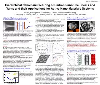
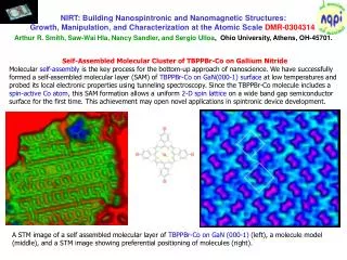
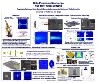
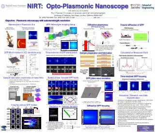
polarizers // to (2, 1) type modes 2.00 • Holographic lithography • Use of chemically amplified negative resist (SU-8) • Precise control of fill factor (easier to make small holes) • Large areas (~ 1 cm2) • E-beam direct write • Tailored structures on same substrate for comparison • Limited area (~ 200 m) Si noise limited spectral measurements Al 1.41 Al on GaAs Au on SiO2 1 m 1.03 200 m 200 m (G-X) (G-X) 0.90 1 m NSF NIRT Grant ECS-068863 PIs: Y. Fainman, V. Lomakin, A. Groisman, and G. W. Schmid-Schoenbeim University of California, San Diego, La Jolla, California 92093-0407 Tel: (858) 534-8909; Fax: (858) 534-1225; E-mail: fainman@ece.ucsd.edu; web site: http://emerald.ucsd.edu Objective: Plasmonic microscopy with sub-wavelength resolution NIRT: Opto-Plasmonic Nanoscope Nanoscope in Plasmonic Era SPP Heterodyne Imaging Setup Diffractive plasmonics: SPP Fresnel Zone Plate Fresnel diffraction of SPP FEM Simulation: Transmission throughSi bumps Microscope: Diffraction limited Plasmonic nanoscope: Sub-diffraction limited Fresnel Zone Plate SPP Fresnel Zone Plate Power Transmission ~ 0.3 Sample illumination CCD Output Fresnel diffraction Input and reference pulse: l0 = 1.55 mm FWHM ~ 200 fs A SPP Fresnel zone plate was fabricated at aluminum (Al)/air interface and worked at the free space wavelength of 1.55 μm (λspp = 1.547μm). The designed focal length was 80 μm. R. Rokitski, KA. Tetz, Y. Fainman, PRL, vol.95, no.17, 21 Oct. 2005, pp.177401/1-4 A 1879 optical microscope Our focusing approach Sub-diffraction limited focusing Time averaged SPP mode* Time-resolved SPP interferogram L. Yin et al, Nano Lett. 5, 1399 (2005) R. Rokitski et al, Phys. Rev. Lett. 95, 177401 (2005) SPP Bloch modes in 2-D nanohole array Calculated vs Measured Field Time evolution of SPP wavepacket Sample preparation and fabrication l~ 1.5 mm, NIR Spatial amplitude and phaseof scattered SPP field Field intensity distribution at the focal plane Measurement Fresnel Diffraction Calculation t = 0 fs t = 133 fs t = 266 fs t = 400 fs Normalized frequency(wa/2pc = a/l) Phase matching condition (resonant Wood’s anomaly): Si-on-Al SPP Fresnel Zone Plate Assuming small modulation (d << a), and no coupling between adjacent sides: Diffraction theory is valid for SPP Ultrafast SPP electrodynamics 20 μm 5 μm (planar case) (-X) Time-resolved SPP focusing Sample fabrication: nanoholes in metal films Spatial phase: focused SPP fields SPP plane wave excitation Snapshots of amplitude at different time Spatial amplitude and phase with converging and diverging illumination • Variety of substrates (GaAs, Si, SiO2, Al2O3) • Evaporation or sputtering of Al, Au, or Ag metallic films (thickness h ~ 50-200 nm) • ICP-RIE and wet etching (hole diameters d ~ 100-500 nm) How to make sure the incident SPP wave is planar? Image without Fresnel zone plate Excitation Array Detection Array Image with Fresnel zone plate Education, Outreach, and Data Dissemination • Established new graduate courses: Nanophotonics (ECE 242A) and Optics in Space and Time (ECE 240B) • Modified Undergraduate Photonics Laboratory in Engineering, Physics and Biochemnistry (opt. comm., CGH, and NLO) • Graduate students weekly meetings and seminars on recent progress and other relevant topics in nanophotonics • Involvement of undergraduate students via NSF’s REU program • Establishing education and outreach projects with the UCSD’s Preuss School, designed for 6-12 grades student coming from disadvantaged households [e. g., Ph.D. students are serving as mentors and leaders of robotics club; RET program with the Undergraduate Photonics Laboratory in Engineering] • Saperstein-2005 JSOE Woolley Fellow, 2006 Summer Graduate Teaching Fellow • Numerous journal publications, conference presentations including invited conference papers • http://emerald.ucsd.edu L. Feng, K. Tetz, B. Slutsky, V. Lomakin, Y. Fainman, Appl. Phys. Lett. 91, 081101 (2007) Imaging various SPP modes R. Rokitski, KA. Tetz, Y. Fainman, Phys. Rev. Lett., vol.95, 2005, pp.177401/1-4 Diffractive SPP focusing Radiative vs. material damping a/l0 SPP focusing after the compensation of radiation loss SPP focusing ASE: = 1520-1570 nm • Simultaneous measurement of both planar and corrugated surface propagation lengths • Determines radiative decay (coupling strength) from grating array Measured focal length: 83μm Designed focal length: 80μm High intensity focused SPP field is observed L. Feng, K. Tetz, B. Slutsky, V. Lomakin, Y. Fainman, Appl. Phys. Lett. 91, 081101 (2007) Fainman Y, Tetz K, Rokitski R, Pang, Optics & Photonics News, vol.17, 24-9, 2006