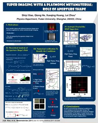
Plasmonic Nanolithography
Plasmonic Nanolithography. EE235 Nanofabrication Jie Yao April 16, 2007. W. Srituravanich, et al, Nano. Lett. 4, 1085 (2004). 2 um. Z. Liu, et al, Nano. Lett. 5, 957, (2005). Light. Surface Plasmons. Higher resolution lithography. Plasmonic Lithography. Plasmonic Nanolithography.

Plasmonic Nanolithography
E N D
Presentation Transcript
Plasmonic Nanolithography EE235 Nanofabrication Jie Yao April 16, 2007
W. Srituravanich, et al, Nano. Lett. 4, 1085 (2004) 2 um Z. Liu, et al, Nano. Lett. 5, 957, (2005)
Light Surface Plasmons Higher resolution lithography Plasmonic Lithography Plasmonic Nanolithography Surface plasmons (SPs) are collective free electron oscillations at a metal/dielectric interface Main features of SPs • Shorter wavelength • (comparing with excitation light) • Evanescent wave enhancement • Bond to the surface • Propagation along the surface H. Raether, Surface Plasmons, (1988).
Hole array lithography W. Srituravanich, et al, Nano. Lett. 4, 1085 (2004)
Glass Al |E| PR substrate Surface Plasmon Interference Surface Plasmon Interference Nanolithography (SPIN) Z. Liu, et al, Nano. Lett. 5, 957, (2005)
(b) Photoresist Al Quartz (c) 0.5 Al 0 2 um Lithography Results (1D) (a) λ0=365nm (d) Photoresist Al Quartz (e) 2 um Period ~115 nm
3μm (b) (a) μm (nm) 8 ~118nm 6 4 2 (c) μm Lithography Results ~60nm Low reflectivity from the slit slit distance doesn’t affect the pattern quality
(d) (c) (b) (a) (d’) (c’) (b’) (a’) (c) 2D SP Interference Lithography • The interference pattern is determined by the arrangement of the SP sources • The resolution is determined by the SP wavelength