Tip-sample interaction, nanoindentation, nanolithography
910 likes | 1.42k Vues
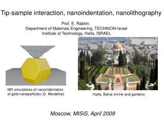
Tip-sample interaction, nanoindentation, nanolithography. Prof. E. Rabkin, Department of Materials Engineering, TECHNION-Israel Institute of Technology, Haifa, ISRAEL. MD simulations of nanoindentation of gold nanoparticles (D. Mordehai). Haifa, Bahai shrine and gardens.

Tip-sample interaction, nanoindentation, nanolithography
E N D
Presentation Transcript
Tip-sample interaction, nanoindentation, nanolithography Prof. E. Rabkin, Department of Materials Engineering, TECHNION-Israel Institute of Technology, Haifa, ISRAEL MD simulations of nanoindentation of gold nanoparticles (D. Mordehai) Haifa, Bahai shrine and gardens Moscow, MISiS, April 2009
Syllabus: -Nanoindentation: main idea and instrumentation; -Introducing load-displacement curve; -What is measured? Olivier-Pharr method; -Calibrating tip radius; -Pile-ups and Joslin-Olivier method; -Indentation size effect: theory of Nix and Gao; -The role of grain boundaries and interfaces; -Nanoindentation with ultralow forces; nanoindenting with AFM; -Nanotribology and nanolithography; -Atomistic theories of tip-sample interaction; -Nanoindenting in the transmission electron microscope; -Applications in biology and medicine.
Vickers microhardness testing Hardness is the property of a material that enables it to resist plastic deformation, usually by penetration. The Vickers microhardness testing method consists of indenting the test material with a diamond indenter, in the form of a right pyramid with a square base and an angle of 136 degrees between opposite faces subjected to a load that does not exceed 1 kgf.
Contact mechanics A contact of a hard sphere with elastic flat specimen: where E* is reduced modulus, or combined modulus of a system The deflection of original surface: The distance of mutual approach: Average pressure:
Elastic-plastic contact For hardness methods that employ the projected contact area, the hardness value,H, is given directly by the mean pressure pm. Experiments show that where sy is the yield stress of the material and C is the constraint factor. For large values of E/sy (metals) C3; For low values of E/sy (glasses) C1.5. Johnson’s “expanding cavity” model: • Indentation response of a material: • pm<1.1sy-fully elastic; • 1.1sy<pm<Csy-plastic deformation • below indenter, but constrained by • surrounding elastic material; • 3. pm>Csy-plastic region extends to • the surface.
Hardness test on the nanoscale The idea of nanoindentation arose from the realization that an indentation test is an excellent way to measure very small volumes of materials. The only problem is determining the indentation area. For the indents below 1 mm in size the resolution of optical microscope is insufficient. To solve this problem depth sensing indentation method was developed. In this method the load and displacement of the indenter are recorded during indentation. Mechanical properties of the indented volume can be determined without seeing the indent. SEM micrograph of the indent made in nc-Cu by Berkovich indenter under the load of 3mN.
Why nanoindentation? Unique mechanics of small volumes (Krystin Van Vilet) Are mechanical properties affected by constraint? Are E, sy, n f(size)? When structure dimensions approach atomic dimensions, is mechanical behavior quantized?
How the nanoindentation testing machine works. Force control The simplest way to apply a controllable low load on the sample is doing this with SFM. The elastic constant of the cantilever beam should be properly characterized. Main disadvantages: -The geometry is not strictly orthogonal; -maximal load is usually in sub-mN range Main advantage: the imaging of the indent is easy.
Other ways of force control Electromagnetic actuation (Micromaterials, NanoIndenter). Main advantages: -Long displacement range (millimeters); -Good P(I) linearity; -High maximal load (few Newtons); -The indenter can be driven in and out. Electrostatic actuation (Hysitron). Main advantages: -Small size, high accuracy; -Good temperature stability; Disadvantages: limited maximal load and displacement. Extremely precise scheme (Burnham and Colton), but not commercially realized.
Displacement control Capacitance method C1-C2 is a linear function of small displacements D. Linear Variable Differential Transducer (LVDT) The primary coil is excited with an a.c. current (1 to 10kHz). The other two coils (the secondaries) are wound such that when a ferritic core (amature) is in the central linear position, an equal voltage is induced into each coil. Robust, cheap, no hysteresis, but lower sensitivity.
Displacement control (continued) Interferometric. Fabry-Perot interferometer. The coherent laser light is channeled through the fiber 1 to fiber 2. It is partly reflected from the back end of fiber 2 and partly transmitted and reflected from the moving mirror. The interference between the beams reflected from the mirror and from the fiber 2 results in periodic variations of the intensity of light at the detector.
Commercial instruments NanoIndenter (MTS, US) http://www.mtsnano.com/f Large maximal load (500 mN); Positioning with the optical microscope.
Hysitron (US) http://www.hysitron.com The advantage of Hysitron is a combination of nanoindenting head with the SPM positioning stage. This allows a precise selection of the object to be tested. The SPM is operating in the STM mode and the Control Unit is “cheated” by providing the voltage from capacitance sensor instead of tunnel current. SPM SPM + Nanoindenter
Micromaterials (UK) http://www.micromaterials.co.uk Original pendulum set-up. Makes high- temperature measurements easier.
Berkovich indenter Berkovich Knoop Cube corner Berkovich indenter was designed to give the same projected area at a given depth as Vickers indenter. It is better suited for small indents.
What is measured? For calculation of nanohardness the knowledge of hc (contact depth at maximal load) is necessary. According to Oliver and Pharr (1992) where e=0.72 for conical indenter and e=0.75 for paraboloid of revolution. S is a contact stiffness.
Oliver-Pharr method Determining machine compliance: Canonical Sneddon stiffness equation: 1. A fraction of unloading curve is fitted with P=A(h-hf)m, where A and m are fitting parameters. 2. The unloading curve fit is differentiated analytically to find the stiffness at maximal load: S=(dP/dh)P=Pmax A series of LARGE indents is made in Al single crystal. The contact area for Berkovich indenter is determined according to Ac=24.5hc2. machine compliance
Determining tip shape area function After machine compliance was found, the empirical tip shape area function is determined Using the set of indents in fused silica: Er=69.6 GPa for diamond indenters. The tip shape area function is determined by fitting the obtained (Ac, hc) data to a poly- nomial of the form: After tip shape area function is determined, the nanohardness is determined according to where The elastic modulus is determined by Sneddon stiffness equation.
Tip radius measurements • Scanning of "calibration grid" (NT-MDT) with the Berkovich indenter: The image of the indenter. • The tip radius: ~400nm.
Max shear stress estimation • The loading response prior to the 1st pop-in can be described as purely elastic loading . • Spherical approximation for the tip (shallow indents) - Hertz theory . • Theoretical shear stress: • homogeneous dislocation nucleation under the indenter.
Common sources of the artifacts -Thermal drift (can be compensated); -Surface preparation (defects and residual deformation); -Tip-sample non-orthogonality and surface roughness; -Incorrect extrapolation of tip area function; -Pile-ups and sink-ins
Nanoindentation gallery Mechanical properties of microstructure elements Mo-22B-11Si T2=Mo5SiB2
Nanoindentation of thin Cu films Pop-ins are especially pronounced in the case of thin films. The stress of the first pop-in is close to the theoretical shear strength of Cu.
Energetics of pop-ins in thin films Elastic energy stored in the film: The interaction energy between two interacting prismatic dislocation loops of radius Rd>>r: The summation over all loops in the film: For the first pop-in in Al film, Rd37 nm.
Measuring mechanical properties of thin films The indentation depth should be less than 1/3 of film thickness. Otherwise, a combination of film and substrate mechanical properties is measured. For “soft” films on hard substrates the Young’s modulus is more sensitive to substrate than the hardness.
Nanoindentation at elevated temperatures C.A. Schuh et al., Nature mater. 4 (2005) 617 Cumulative distributions:
Nanoindentation at elevated temperature: data analysis Activation volume obtained: 0.5b3 Not consistent with homogeneous nucleation Role of vacancies? The model also predicts rate dependence of the pop-in load
Nanoindentation creep Voigt, spherical indenter: Maxwell, spherical indenter: Voigt (a), Maxwell (b) and combined (c) models of visco-elastic creep. Voigt fit 1 mm thick Al film, spherical indenter
Diffusion creep For loads lower than the first pop-in stress exponent is 1.5 at the end of holding period. This is close to the exponent 1 expected from diffusion mechanism. Load-displacement curve for In at room temperature
The pile-ups Stress-strain relationship in the plastic region: for Piling-up is expected for non strain- hardening materials with large E/sy (heavily deformed metals). Sinking-in is more likely to occur in materials with small E/sy (ceramics, glasses). In the case of extensive piling-up or sinking-in determing the correct value of nanohardness is difficult
Example of pile-ups (1) (a)-(c): Nanocrystalline Cu obtained by severe plastic deformation; (d)-annealed Cu polycrystal. 3 mN load.
Joslin-Oliver method Using Sneddon relationship allows eliminating projected area from the expression for nanohardness: The method is good when the elastic modulus is known with high accuracy. Eliminates the effect of pile-ups, surface roughness and indenter shape area function.
Indentation size effect For low loads hardness is a strong function of the indentation depth. Therefore, there is little sense in direct comparison of hardness values. A good way to get the FULL H(d) dependence in one indentation run is the use of partial unloading technique. loading schedule: Partial unloading scheme
Theory of Nix and Gao Geometry: Total length of dislocation loops in plastic hemisphere: Density of geometrically necessary dislocations: Taylor’ relation for shear strength: where a 0.5 and H=3sy we get: With von Mises flow rule
The effect of grain boundaries Local hardening in the sub-um range
Grain boundary hardness in Ni3Al Wo & Ngan, J. Mater. Res., 2003 Cube corner indenter, 300 mN max. load It was concluded that no grain boundary hardening effect can be observed in nanoindentation experiment
Truncated hemisphere model T. Eliash, E. Rabkin, Acta mater., 2008
Ultra-microhardness of Zn at different loads Muktipavela et al, J. Mater. Sci., 2008 Grain boundaries stop the deformation twinning
Inverse size effect Yang & Vehoff, Acta mater., 2007
AFM as a force measuring apparatus Frictional (lateral) force microscopy Twisting of cantilever during scanning can be used to measure the frictional force Ff. Amontons’ law: m is the friction coefficient. Cantilever twist can be measured either using capacitance method (a) or optically with quadrant PSD (b). FFM image of gold islands deposited on organic-coated mica. Au exhibits low friction.
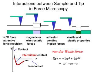
Force spectroscopy Experimentally measured: zt – cantilever deflection; zs – sample movement. attraction The force, F: The relative displacement of tip and sample, s: “jump to contact” repulsion zt(zs) = F(s) 1-maximal attractive force; 3-maximal adhesive force
Humidity and contaminations in force spectroscopy In vacuum In humid air and with contaminations
Example of adhesion curve -Maps of attractive and adhesive forces; -The slope of the curve after contact is established gives an information on local atomic forces; -Hysteresis is a measure of inelasticity in the tip-sample system. TaS2 vs. SiO2 cantilever (E. Meyer, 1990)
Nanoindentation with AFM Non-Hertzian behavior because penetration depth is comparable with the tip radius: Indented with Si tip, R<10 nm (J. Fraxedas et al., PNAS 2002)
Spatial maps of surface elasticity Input: periodic modulation of zs. Measured: caused by it periodic changes of zt cs and c-effective spring constant of the surface and of cantilever, respectively. Cantilever should be selected properly! 32 mm2 topography (a) and modulus map (b) images of epoxy-carbon fiber composite (Maivald et al., 1991)
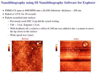
Nanolithography with AFM Sundararajan & Bhushan, J. Mater. Res., 2001 Most commercial AFMs are equipped with the nanolithography software which enables controlled “plowing” of the surface Scratch test of Si (001) surface, with monotonously increasing normal force and friction force continuously monitored. Rapid increase in friction force corresponds to the wear groove formation.