Download
1 / 42
450 likes | 941 Vues
Types of Nanolithography. Types of Lithography. A. Photolithography (optical, UV, EUV) B. E-beam/ion-beam/Neutral atomic beam lithography C. X-ray lithography D. Interference lithography E. Scanning Probe Voltage pulse CVD Local electrodeposition

E N D
Types of Lithography • A. Photolithography (optical, UV, EUV) • B. E-beam/ion-beam/Neutral atomic beam lithography • C. X-ray lithography • D. Interference lithography • E. Scanning Probe Voltage pulse CVD Local electrodeposition Dip-pen F. Step Growth G. Soft Lithography H. Nanoimprint I. Shadow Mask J. Self-Assembly K. Nanotemplates Diblock copolymer Sphere Alumina membrane Nanochannel glass Nuclear-track etched membrane
II-A. Photolithography • KrF λ=248nm • ArF λ=193nm • F2 λ=157nm
II-B. Electron-Beam Lithography • Exposure source: electron beam • At acceleration voltage Vc=120kV, λ=0.0336Å • Utilizes an electron column to generate focused e-beam
SEM Resolution • Magnification x Resolution in (Å) = 107 for a 1mm feature on the image • Collimation • Wavelength • Charging effect - coating carbon, metal thickness • Escape depth metal ~40 Å semiconductor ~100 Å insulator ~300 Å
E – Beam Writing • Advantages Better resolution Direct writing, no mask needed Arbitrary size, shape, order • Disadvantages Serial process slow, small area Compatibility conducting, no high T process
Sample E-beam Writing Procedure • Application of e-beam resist (PMMA) • Spin coating & soft bake • Loading Ag paint reference, position • Power on • Tuning emission current • Stabilizing filament • Gun alignment • Adjust astigmatism • Referencing • Focusing • Writing • Shutting down SEM • Developing • Hard bake
II-C. X-ray Lithography • Exposure source: x-ray (synchrotron) • Resist: sensitive to x-ray (PMMA) – IBM used resists developed for DUV and obtained successful results • Mask: SiC membrane covered by high Z metal; fabricated by e – beam writer • Advantages: High resolution • Large area • Disadvantage: Synchrotron facility necessary
X- Ray Lithography: Applications • IC industry – Proposed for fabricating Gigabit-level DRAM – Not a mainstream technique for IC fabrication • Nanoelectronics • MEMS applications • – LIGA • – High aspect ratio devices
Conclusions • Electron-beam lithography is currently the industry standard for high-resolution, but has limited applications due to its high cost and time-demanding process. • X-ray lithography is an up-and-coming technology that can be used in the same capacities as optical lithography with better results. However, due to the high cost of the equipment and supplies, as well as the desire to push optical lithography to its absolute limit, we can only say that x-ray lithography has a bright future ahead.
References for E – Beam and X – Ray Lithography • C. Ngo and C. Rosilio, "Lithography for semiconductor technology," Nucl. Instr. and Meth. In Phys. Res. B, vol. 131, pp. 22-29, 1997. • R. C. Jager, Introduction to Microelectronic Fabrication, vol. 5. Upper Saddle River, New Jersey: Prentice Hall, 2002. • J. G. Chase and B. W. Smith, "Overview of Modern Lithography Techniques and a MEMS Based Approach to High Throughput Rate Electron Beam Lithography," J. Intell. Mater. Syst. Struct., vol. 12, pp. 807-817, 2002. • J. N. Helbert, Handbook of VLSI Microlithography. Norwich, NY: Noyes Publications/William Andrew Publishing, LLC., 2001. • "Facility Procedures," in http://rlewb.mit.edu/sebl/facility_procedures.htm. • "Raith Nanolithography Products," in http://www.raith.com/WWW_RAITH/nanolithography/nano_faqs2.html. • "Electron Beam Lithography," in http://www.shef.ac.uk/eee/research/ebl. • K.-S. Chen, I.-K. Lin, and F.-H. Ko, "Fabrication of 3D Polymer Microstructures Using Electron Beam Lithography and Nanoimprinting Technologies," J. Micromech. Microeng., vol. 15, 2005. • • J. P. Silverman, "Challenges and Progress in X-ray Lithography," J. Vac. Sci. Technol. B, vol. 16, pp. 3137-3140, 1998. • • S. Ohki and S. Ishihara, "An Overview of X-ray Lithography," Microelectron. Eng., pp. 171-178, 1996.
Focused Ion Beam (FIB) • Liquid ion source: Ga, Au-Si-Be alloys LMI sources due to the long lifetime and high stability. • Advantages: • High exposure sensitivity: 2 or more orders of magnitude higher than that of electron beam lithography • Negligible ion scattering in the resist • Low back scattering from the substrate • Can be used as physical sputtering etch and chemical assisted etch. • Can also be used as direct deposition or chemical assisted deposition, or doping . • Disadvantages: • Lower throughput, extensive substrate damage.
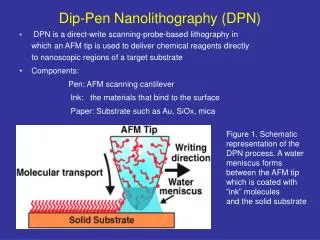
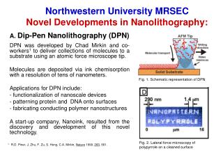
II-E. Scanning Probe Lithography • Probe STM, AFM • Techniques Voltage pulse CVD Local electrodeposition Dip-pen
Two Different Modes of STM • Constant current mode • Constant height mode
Manipulation of Atoms • Parallel process • Perpendicular process
Nanolithography • Local anodic oxidation, passivation, localized chemical vapor deposition, electrodeposition, mechanical contact of the tip with the surface, deformation of the surface by electrical pulses
Thermal Dip Pen Lithography Diagram illustrating thermal dip pen nanolithography. When the cantilever is cold (left) no ink is deposited. When the cantilever is heated (right), the ink melts and is deposited onto the surface. (Journal of the American Chemical Society,128(21) pp 6774 - 6775 , 2006)
Thermal Dip Pen Lithography • To perform the tDPN technique, the team employed a silicon cantilever that contained a resistive heater and had a radius of curvature at its tip of about 100 nm. As the ink they used octadecylphosphonic acid (OPA), a material that has a melting point of 99 °C and self-assembles into monolayers on mica, stainless steel, aluminium and oxides such as titania and alumina. Sheehan and colleagues coated the cantilever with OPA before heating it to 122 °C to melt the ink. Scanning the tip across a mica substrate laid down 98 nm wide lines of OPA. • The scientists were able to stop depositing molecules from the cantilever by turning off the current supply to the resistive heater. That said, it took around two minutes for the deposition process to stop, perhaps because of the low thermal conductivity of the mica substrate. • The researchers believe that optimizing the technique, for example by decreasing the radius of curvature of the cantilever tip, should enable them to deposit features around 10 nm in size. So tDPN could find applications in producing features too small to be formed by photolithography, as a nanoscale soldering iron for repairing circuits on semiconductor chips, or for making bioanalytical arrays. (Paul Sheehan, Lloyd Whitman, Applied Physics Letters, Sep. 10, 2004)
Thermal Dip Pen Lithography – Conducting Polymer • Whitman and colleagues Minchul Yang, Paul Sheehan and Bill King deposited layers of the conducting polymer poly(3-dodecylthiophene) (PDDT) onto silicon oxide surfaces. They produced nanostructures with lateral dimensions of less than 80 nm and achieved monolayer-by-monolayer thickness control – a monolayer of the molecules was around 2.6 nm thick. The researchers were also able to control the orientation of the polymer chains. • PDDT has promise in the field of organic electronics and could have applications in areas such as transistors, photovoltaic devices and video displays. "The performance of these devices depends critically on the degree of molecular ordering and orientation within the polymer film, a property that has been difficult to control," said Whitman. "We have succeeded in directly writing polymer nanostructures with monolayer-by-monolayer thickness control using tDPN. The deposition process employs highly local heating to produce this polymer ordering and orientation."
A dip-pen nanolithography that has an array of 55,000 pens that can create 55,000 identical molecular patterns The background shows some of the 55,000 miniature images of a 2005 US nickel made with dip-pen lithography. (Each circle is only twice the diameter of a red blood cell.) Each nickel image with Thomas Jefferson's profile (in red) is made of a series of 80 nm dots. The inset (right) is an electron microscope image of a portion of the 55,000-pen array (Angewandte Chemie45 1-4, 2006 )