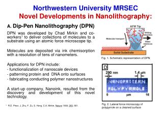
html5-img
1 / 8

Nanolithography using DI Nanolithography Software for Explorer

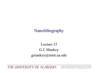
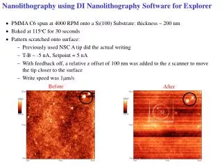
Before. After. Nanolithography using DI Nanolithography Software for Explorer. PMMA C6 spun at 4000 RPM onto a Si(100) Substrate: thickness ~ 200 nm Baked at 115 o C for 30 seconds Pattern scratched onto surface: Previously used NSC A tip did the actual writing T-B ~ -5 nA, Setpoint = 5 nA

aspen
Télécharger la présentation

Nanolithography using DI Nanolithography Software for Explorer

An Image/Link below is provided (as is) to download presentation Download Policy: Content on the Website is provided to you AS IS for your information and personal use and may not be sold / licensed / shared on other websites without getting consent from its author. Content is provided to you AS IS for your information and personal use only. Download presentation by click this link. While downloading, if for some reason you are not able to download a presentation, the publisher may have deleted the file from their server. During download, if you can't get a presentation, the file might be deleted by the publisher.

E N D

Presentation Transcript


  1. Before After Nanolithography using DI Nanolithography Software for Explorer • PMMA C6 spun at 4000 RPM onto a Si(100) Substrate: thickness ~ 200 nm • Baked at 115oC for 30 seconds • Pattern scratched onto surface: • Previously used NSC A tip did the actual writing • T-B ~ -5 nA, Setpoint = 5 nA • With feedback off, a relative z offset of 100 nm was added to the z scanner to move the tip closer to the surface • Write speed was 1mm/s

  2. Nanolithography: OU Symbol

  3. Nanolithography: OU Symbol - Zoom in

  4. Nanolithography: OU Symbol - Line Scan

  5. Nanolithography: OU Symbol - 3D View

  6. Nanolithography: Luke -first write

  7. Nanolithography: Vertical and Horizontal lines

  8. Nanolithography: Tip image Before and After

More Related