1. Crystal Structure
1. Crystal Structure. Issues that are addressed in this chapter include: Periodic array of atoms Fundamental types of lattices Index system for crystal planes Simple crystal structures Imaging of atomic structure Non-ideal structures. 1.1 Periodic Array of Atoms.


1. Crystal Structure
E N D
Presentation Transcript
1. Crystal Structure Issues that are addressed in this chapter include: • Periodic array of atoms • Fundamental types of lattices • Index system for crystal planes • Simple crystal structures • Imaging of atomic structure • Non-ideal structures EEE539 Solid State Electronics
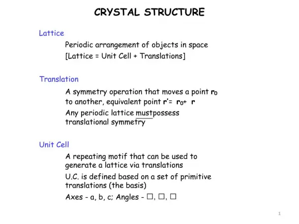
1.1 Periodic Array of Atoms Crystals are composed of a periodic array of atoms: • The structure of all crystals can be described in terms of a lattice, with a group of atoms attached to each lattice point called basis: basis + lattice = crystal structure + = EEE539 Solid State Electronics
The lattice and the lattice translation vectors a1, a2, and a3 are primitive if any two points satisfy: where u1, u2 and u3 are integers. • The primitive lattice translation vectors specify unit cell of smallest volume. • A lattice translation operator is defined as a displacement of a crystal with a crystal translation operator. • To describe a crystal, it is necessary to specify three things: • What is the lattice • What are the lattice translation vectors • What is the basis EEE539 Solid State Electronics
A basis of atoms is attached to a lattice point and each atom in the basis is specified by: where 0 xj, yj, zj 1. The basis consists of one or several atoms. • The primitive cell is a parallelepiped specified by the primitive translation vectors. It is a minimum volume cell and there is one lattice point per primitive cell. • The volume of the primitive cell is: • Basis associated with a primitive cell is called a primitive basis and contains the least # of atoms. EEE539 Solid State Electronics
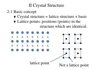
1.2 Fundamental types of lattices To understand the various types of lattices, one has to learn elements of group theory: • Point group consists of symmetry operations in which at least one point remains fixed and unchanged in space. There are two types of symmetry operations: proper and improper. • Space group consists of both translational and rotational symmetry operations of a crystal. In here: T = group of all translational symmetry opera- tions R = group of all symmetry operations that involve rotations. EEE539 Solid State Electronics
The most common symmetry operations are listed below: • C2 = two-fold rotation or a rotation by 180° • C3 = three-fold rotation or a rotation by 120° • C4 = four-fold rotation or a rotation by 90° • C6 = six-fold rotation or a rotation by 180° • s = reflection about a plane through a lattice point • i = inversion, I.e. rotation by 180° that is followed by a reflection in a plane normal to rotation axis. • Two-dimensional lattices, invariant under C3, C4 or C6 rotations are classified into five categories: Oblique lattice Special lattice types (square, hexagonal, rectangular and centered rectangular) EEE539 Solid State Electronics
Three-dimensional lattices – the point symmetry operations in 3D lead to 14 distinct types of lattices: • The general lattice type is triclinic. • The rest of the lattices are grouped based on the type of cells they form. • One of the lattices is a cubic lattice, which is further separated into: • simple cubic (SC) • Face-centered cubic (FCC) • Body-centered cubic (BCC) • Note that primitive cells by definition contain one lattice point, but the primitive cells of FCC lattice contains 4 atoms and the primitive cell of BCC lattice contains 2 atoms. EEE539 Solid State Electronics
The primitive translation vectors for cubic lattices are: simple cubic face-centered cubic body-centered cubic EEE539 Solid State Electronics
1.3 Index System for Crystal Planes – Miler Indices The orientation of a crystal plane is determined by three points in the plane that are not collinear to each other. It is more useful to specify the orientation of a plane by the following rules: • Find the intercepts of the axes in terms of lattice constants a1, a2 and a3. • Take a reciprocal of these numbers and then reduce to three integers having the same ratio. The result (hkl) is called the index of a plane. • Planes equivalent by summetry are denoted in curly brackets around the indices {hkl}. EEE539 Solid State Electronics
Miller indices for direction are specified in the following manner: • Set up a vector of arbitrary length in the direction of interest. • Decompose the vector into its components along the principal axes. • Using an appropriate multiplier, convert the component values into the smallest possible whole number set. [hkl] – square brackets are used to designate specific direction within the crystal. <hkl> - triangular brackets designate an equivalent set of directions. EEE539 Solid State Electronics
The calculation of the miller indices using vectors proceeds in the following manner: • We are given three points in a plane for which we want to calculate the Miller indices: P1(022), P2(202) and P3(210) • We now define the following vectors: r1=0i+2j+2k, r2=2i+0j+2k, r3=2i+j+0k and calculate the following differences: r - r1=xi + (2-y)j + (2-z)k r2 - r1=2i - 2j + 0k r3-r1 = 2i – j - 2k • We then use the fact that: (r-r1).[(r2-r1) ×(r3-r1)] =A.(B×C)= 0 EEE539 Solid State Electronics
We now use the following matrix representation, that gives The end result of this manipulation is an equation of the form: 4x+4y+2z=12 • The intercepts are located at: x=3, y=3, z=6 • The Miller indices of this plane are then: (221) EEE539 Solid State Electronics
The separation between adjacent planes in a cubic crystal is given by: The angle between planes is given by: EEE539 Solid State Electronics
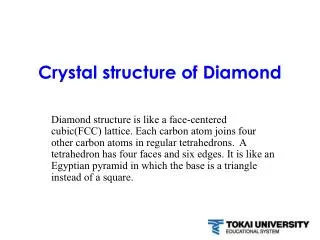
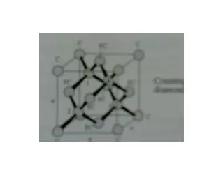
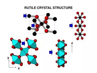
1.4 Simple Crystal Structures There are several types of simple crystal structures: • Sodium Chloride (NaCl) -> FCC lattice, one Na and one Cl atom separated by one half the body diagonal of a unit cube. • Cesium Chloride -> BCC lattice with one atom of opposite type at the body center • Hexagonal Closed packed structure (hcp) • Diamond structure -> Fcc lattice with primitive basis that has two identical atoms • ZnS -> FCC in which the two atoms in the basis are different. EEE539 Solid State Electronics
1.5 Imaging of Atomic Structure The direct imaging of lattices is accomplished with TEM. One can see, for example, the density of atoms along different crystalographic directions. EEE539 Solid State Electronics
1.6 Non-ideal Crystal Structures There are two different types of non-idealities in the crystalline structure: • Random stacking – The structure differs in stacking sequence of the planes. For example FCC has the sequence ABCABC …, and the HCP structure has the sequence ABABAB … . • Polytypism – The stacking sequence has long repeat unit along the stacking axis. • Examples include ZnS and SiC with more than 45 stacking sequences. • The mechanisms that induce such long range order are associated with the presence of spiral steps due to dislocations in the growth nucleus. EEE539 Solid State Electronics