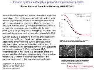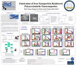
Nanocomposites Overview Electron Microscopy of Nanocomposites
Electron Microscopy of Nanocomposites. Outline. Nanocomposites Overview Electron Microscopy of Nanocomposites. Nanostructures. Nanostructures : structures with at least one dimension on the order of 1-100 nm

Nanocomposites Overview Electron Microscopy of Nanocomposites
E N D
Presentation Transcript
Electron Microscopy of Nanocomposites Outline • Nanocomposites Overview • Electron Microscopy of Nanocomposites
Nanostructures • Nanostructures: structures with at least one dimension on the order of 1-100 nm • Nanostructure properties differ from bulk (i.e. atomic ionization, chemical reactivities, magnetic moments, polarizabilities, geometric structures, etc.) • Nanostructures have the potential to be evolutionary (ICs) as well as revolutionary (Quantum Computing)
Nanocomposites Overview • Nanocomposites are a broad range of materials consisting of two or more components, with at least one component having dimensions in the nm regime (i.e. between 1 and 100 nm) • Typically consists of a macroscopic matrix or host with the addition of nanometer-sized particulates or filler • Filler an be: 0 D (nano-particles), 1 D (nano-wires, nano-tubes), 2 D (thin film coatings, quantum wells), or 3 D (embedded networks, co-polymers) • e.g. CNTs in a polymer matrix
Nanocomposites • Resulting nanocomposite may exhibit drastically different (often enhanced) properties than the individual components • Electrical, magnetic, electrochemical, catalytic, optical, structural, and mechanical properties Lycurgus Cup Lycurgus Cup is made of glass. Roman ~400 AD, Myth of King Lycurgus Appears green in reflected light and red in transmitted light http://www.thebritishmuseum.ac.uk/science/lycurguscup/sr-lycugus-p1.html
Nanocomposites • Technology re-discovered in the 1600s and used for colored stained glass windows The Institute of Nanotechnology http://www.nano.org.uk/
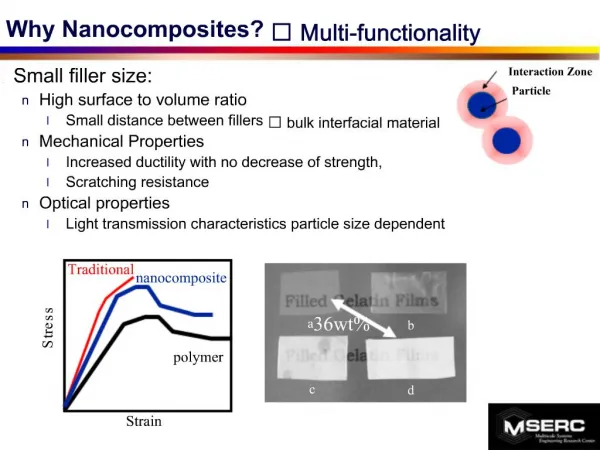
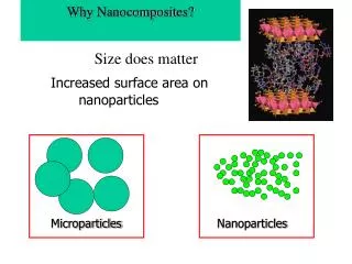
Nanocomposites Why Nano? • Very high surface area to volume ratios in nanostructures • Nanocomposites provide large interface areas between the constituent, intermixed phases • Allow significant property improvements with very low loading levels (Traditional microparticle additives require much higher loading levels to achieve similar performance) • Apart from the properties of the individual components in a nanocomposite, the interfaces play an important role in enhancing or limiting overall properties of system • Controls the degree of interaction between the filler and the matrix and thus influences the properties • Alters chemistry, polymer chain mobility, degree of cure, crystallinity, etc.
Nanostructure Properties Surface to Volume Ratio Si Cube with (100)-Directed Faces • Surface and interface properties (e.g. adhesive and frictional forces) become critical as materials become smaller • High surface area materials have applications in: energy storage, catalysis, battery/capacitor elements, gas separation and filtering, biochemical separations, etc.
Nanocomposites Other Properties and Benefits • Interaction of phases at interface is key: • Adding nanotubes to a polymer can improve the strength (due to superior mechanical properties of the NTs) • A non-interacting interface serves only to create weak regions in the composite resulting in no enhancement • Most nano-particles do not scatter light significantly • Possible to make composites with altered electrical or mechanical properties while retaining optical clarity • CNTs and other nano-particles are often essentially defect free
Nanocomposites and Potential Applications Nanoclays in Polymers • Liquid and Gaseous barriers • Oxygen transmission for polyamide-organoclay composites usually less than half that of unmodified polymer • Food packaging applications (processed meats, cheese, cereals) to enhance shelf life • Reduce solvent transmission through polymers such as polyamides for fuel tank and fuel line components • Reduce water absorption in polymers (environmental protection) • Reduction of flammability of polymeric materials (e.g. polypropylene) with as little as 2% nanoclay loading Nanotubes in Polymers • High strength materials • Modulus as high as 1 TPa and strengths as high as 500 GPa • Significant weight reductions for similar performance, greater strength for similar dimensions (military and aerospace applications) • Electrically conductive polymers
Nanocomposites Characterization Techniques Tools of the Trade • Several techniques used for nanocomposites including: • Nuclear Magnetic Resonance • Neutron Scattering Methods • X-Ray Diffraction • Atomic Force Microscopy • Scanning Electron Microscopy • Transmission Electron Microscopy • Transmission Electron Microscopy and X-ray Diffraction are the most common techniques
SEM Capabilities Backscattered Imaging (BSI) Secondary Electron Imaging (SEI) • Surface Topography, Morphology, Particle Sizes, etc. • Compositional Contrast Scanning Electron Microscope (SEM) Transmitted Electron Imaging (TEI) Electron Backscattered Electron Diffraction (EBSD) • Internal ultrastructure Energy-Dispersive X-ray Spectrometry (EDS) • Crystallographic Info • Elemental composition, mapping and linescans
TEM Capabilities Electron Diffraction (ED) Bright- and Dark-Field Imaging (BF/DF imaging) • Crystallographic Info • • Internal ultrastructure • Nanostructure dispersion • Defect identification Transmission Electron Microscope (TEM) High-Resolution Transmission Electron Microscopy (HR-TEM) Electron Energy Loss Spectroscopy (EELS) • • Chemical composition • Other Bonding info • Interface structure • Defect structure Energy-Dispersive X-ray Spectrometry (EDS) • Elemental composition, mapping and linescans
Electron Microscopy of Nanocomposites Layered Silicates (Nanoclay) and Polymer Nanocomposites • Improved properties related to the dispersion and nanostructure (aspect ratio, etc.) of the layered silicate in polymer • The greatest improvement of these benefits often comes with exfoliated samples • Intercalate: Organic component inserted between the layers of the clay • Inter-layer spacing is expanded, but the layers still bear a well-defined spatial relationship to each other • Exfoliated: Layers of the clay have been completely separated and the individual layers are distributed throughout the organic matrix • Results from extensive polymer penetration and delamination of the silicate crystallites http://www.azom.com/details.asp?ArticleID=936
Polymer-Layered Silicate Nanocomposites TEM of Intercalated Nanoclay • Organoclay nanocomposite (10% in Novalac-Based Cyanate Ester) • XRD gives average interlayer d-spacing while TEM can give site specific morphology and d-spacing • In this case, XRD gave no peaks • Many factors such as concentration and order of the clay can influence the XRD patterns • XRD often inconclusive when used alone Alexander B. Morgan, and Jeffrey W. Gilman, “Characterization of Polymer-Layered Silicate (Clay) Nanocomposites by Transmission Electron Microscopy and X-Ray Diffraction: A Comparative Study”, J. Applied Polymer Science, 87 1329-1338 (2003).
Polymer-Layered Silicate Nanocomposites TEM Image of an Intercalated/Exfoliated PS Nanocomposite • In the author’s own words: • “The majority of PLSNs that we investigated were best described as intercalated/exfoliated. By XRD, they would be simply defined as intercalated, in that there was an observed increase in the d-spacing as compared to the original clay d-spacing. However, the TEM images showed that although there were indeed intercalated multilayer crystallites present, single exfoliated silicate layers were also prevalent, hence, the designation of an intercalated/exfoliated type of PLSNs.” Small Intercalated Clay Layers Exfoliated Single Layers Alexander B. Morgan, and Jeffrey W. Gilman, “Characterization of Polymer-Layered Silicate (Clay) Nanocomposites by Transmission Electron Microscopy and X-Ray Diffraction: A Comparative Study”, J. Applied Polymer Science, 87 1329-1338 (2003).
Epoxy-Based Clay Nanocomposites TEM Images of Clay/Epoxy Nanocomposites • Change of basal spacing of organo-clay nanocomposites during processing of epoxy/clay nanocomposites by the sonication technique • TEM images of nanoclay in different epoxy systems showing intercalated(white arrows)/exfoliated (black arrows) nanocomposite hybrids • Increase in basal d-spacings in nanoclay platelets observed by TEM and XRD • In some cases from 1.8 nm up to 8.72 nm Hiroaki Miyagawa, Lawrence T. Drzal, and Jerrold A. Carsello, “Intercalation and Exfoliation of Clay Nanoplatelets in Epoxy-Based Nanocomposites: TEM and XRD Observations”, Polymer Engineering and Science, 46(4) 452-463 (2006).
Carbon Nanotube/Polymer Nanocomposites Surface and cross-sectional SEM images of (5 wt % SWNTs)/polystyrene composite film • SWNTs solubilized in chloroform with poly(phenyleneethynylene)s (PPE) along with vigorous shaking and/or short bath sonication • The functionalized SWNT solution mixed with a host polymer (polycarbonate or polystyrene) solution in chloroform to produce a nanotube/polymer composite solution • Composite film prepared from this solution on a silicon wafer either by drop casting or by slow-speed spin coating R. Ramasubramaniama, J. Chen, and H. Liu, “Homogeneous Carbon Nanotube Polymer Composites for Electrical Applications”, J. Appl. Phys., 83 2928-2930 (2003).
Carbon Nanotube/Polymer Nanocomposites • The conductivity of pure polystyrene is about 10-14 S/m (The conductivity of pristine HiPCO-SWNT buckypaper is about 5.1X10⁴ S/m) • Conductivity of composite increases sharply between 0.02 and 0.05 wt% SWNT loading indicating the formation of a percolating network • Rapid increase in electrical conductivity of composite materials takes place when the conductive filler forms an infinite network of connected paths through the insulating matrix R. Ramasubramaniama, J. Chen, and H. Liu, “Homogeneous Carbon Nanotube Polymer Composites for Electrical Applications”, J. Appl. Phys., 83 2928-2930 (2003).
Graphene-Based Polymer Nanocomposites 1 mm 500 nm SEM Images of 2.4 Vol % Graphene Nanocomposites • Polystyrene/chemically modified graphene composite made by solution based processing technique followed by hot pressing or injection molding to form continuous specimens • SEM images shows sheets of graphene are crumpled, wrinkled, and at times folded • At 2.4 Vol % the composite appears to be almost entirely filled with the graphene sheets even though 97.6 Vol % is still filled by the polymer • This visual effect is due to the enormous surface area of the sheets Sasha Stankovich, Dmitriy A. Dikin, Geoffrey H. B. Dommett, Kevin M. Kohlhaas, Eric J. Zimney, Eric A. Stach, Richard D. Piner, SonBinh T. Nguyen, and Rodney S. Ruoff, Graphene-Based Composite Materials”, Nature 442 282-286 (2006).
Graphene-Based Polymer Nanocomposites HRTEM and SAED Patterns of Graphene Nanocomposites 10 nm 10 nm • TEM used to determine if the graphene-based sheets were present as exfoliated sheets or multi-layered platelets • Electron diffraction patterns and d spacings as well as high resolution TEM suggest that platelets are individual graphene sheets randomly dispersed in the polymer matrix • High resolution TEM shows regions where fringes are observed and regions where they are not indicating significant local curvature in the graphene sheets Sasha Stankovich, Dmitriy A. Dikin, Geoffrey H. B. Dommett, Kevin M. Kohlhaas, Eric J. Zimney, Eric A. Stach, Richard D. Piner, SonBinh T. Nguyen, and Rodney S. Ruoff, Graphene-Based Composite Materials”, Nature 442 282-286 (2006).
Graphene-Based Polymer Nanocomposites • Percolation threshold occurs when the filler concentration is near 0.1 Vol % • This is about 3 times lower than that reported for any other 2D filler • Due to extremely high aspect ratio of the graphene sheets and homogeneous dispersion in the composites • Electrical properties compare well with values reported in the literature for nanotube/polymer composites • Graphene have higher surface-to-volume ratios due to inaccesibility of inner nanotube surface to polymer molecules • SWNTs still much more expensive than graphite Sasha Stankovich, Dmitriy A. Dikin, Geoffrey H. B. Dommett, Kevin M. Kohlhaas, Eric J. Zimney, Eric A. Stach, Richard D. Piner, SonBinh T. Nguyen, and Rodney S. Ruoff, Graphene-Based Composite Materials”, Nature 442 282-286 (2006).
Nano-Capacitors Nano-Capacitor Device Schematic • Nano-Capacitors grown using anodic aluminum oxide templates and reactive ion etching to transfer nano-hole pattern into underlying substrate
Nano-Capacitors Top Down SEM of SiO2 Oblique Angle SEM • SEM images before nitride etch and oxide growth • Samples without nitride buffer layer resulted in rounded profiles
Nano-Capacitors Room Temperature C-V • Both poly Si gated and electroylyte gated configurations showed little leakage at room temperature • Gated-Si area is major contribution to the capacitance
Nano-Batteries: Teeters Battery Based on existing work at Tulsa • Anopore™ membrane • Disordered cells • Carbon dust anode particles • Reducing the size of battery electrodes to the nanoscale allows their use in autonomous nanodevices • Nanoscale electrode materials typically show higher capacities, lower resistance, and lower susceptibility to slow electron-transfer kinetics than standard electrode configurations Electrolyte: PEO/ Li Triflate wax Cathode: Sputtered LiCoO2 Anode: Carbon, Tin Oxide, or ITO
Nano-Batteries: Electrolyte-Filled Pores Filled “Air" Pockets? Empty Empty Pockets
Nano-Batteries: Anode Particles Tin Oxide Ion Milling Tin Oxide Polishing Carbon Polishing
Our JEOL 2010F Field Emission TEM Au (100) • TEM Lattice Resolution: 0.102 nm • 200 kV, Mag.= 1,500,000X, Bright Field Image
Our JEOL 2010F Field Emission TEM Si (110) • High Angle Annular Dark Field STEM Resolution: 0.136 nm • 200 kV, Mag.= 8,000,000X, Spot Size = 0.2 nm Filtered Image of red square area
Polymer-Layered Silicate Nanocomposites • Consideration of architecture (cyclic vs. linear) and kinetics (medium viscosity and shear) is critical for nanocomposite formation • Important consequence of the charged nature of the clays is that they are generally highly hydrophilic and therefore incompatible with a wide range of polymer types • Organophilic clay can be produced by ion exchange with an organic cation • e.g. in Montmorillonite the sodium ions in the clay can be exchanged for an amino acid such as 12-aminododecanoic acid (ADA) to make clay hydrophobic and potentially more compatible with polymers • Modifiers used for the layered silicate that participate in the polymerization (functional groups such as initiators, comonomers, and chain transfer agents) • Suggested that these participating modifiers create tethered polymer chains that maintain stable exfoliation before and after melt processing • Often silicate (not organically modified) added in post polymerization step • Latex particles have cationic surface charges (arising from choice of emulsifier) and the silicate layers have anionic charges, electrostatic forces promote an interaction between the silicate and polymer particles
Polymer-Layered Silicate Nanocomposites • Platelet thickness ~ 1nm, aspect ratios ~ 100-1500, and surface areas ~ 200 m2/gram • Important to understand the factors which affect delamination of the clay: ion-dipole interactions, use of silane coupling agents and use of block copolymers • Example of ion-dipole interactions is the intercalation of a small molecule such as dodecylpyrrolidone in the clay. Entropically-driven displacement of the small molecules then provides a route to introducing polymer molecules • Unfavourable interactions of clay edges with polymers can be overcome by use of silane coupling agents to modify the edges • Block copolymers: One component of the copolymer is compatible with the clay and the other with the polymer matrix
SEM Sample Preparation SEM Sample Considerations • What form or condition is the sample in? • Is the size of the sample compatible with the chamber? • Bulk specimen, thin film (un-supported?), fibers, powders, particles • Wet or dry? • Is high vacuum okay for the sample? • Conductive or Insulating? SEM Sample Requirements • Conventional SEM sample requirements: • Clean • Dry • Conductive • Conductive path to ground (usually through sample stub)
SEM Sample Mounting • No standard SEM sample holder or stub • Usually made of aluminum, brass, or copper
Sputter Coating for Sample Conductivity • Target material (typically AuPd alloy, Ir, etc.) exposed to an energized gas plasma • Gas plasma is usually an inert gas such as Ar • Target surface is eroded by the plasma and atoms are ejected • Atoms collide with residual gas molecules and deposit everywhere in chamber • Provides a multidirectional coating on a stationary specimen
TEM Specimen Preparation Specimen Requirements • Specimen must be thin enough to transmit sufficient electrons to form an image (100 nm) • It should be stable under electron bombardment in a high vacuum • Must fit the specimen holder (i.e. < 3 mm in diameter) • Ideally, specimen preparation should not alter the structure of the specimen at a level observable with the microscope • Always research (i.e. literature search) the different methods appropriate for your sample prep first
TEM Grids • 3 mm diameter (Nom. 3.05 mm) grids used for non self-supporting specimens • Specialized grids include: • Bar grids • Mixed bar grids • Folding grids (Oyster grids) • Slot grids • Hexagonal grids • Finder grids • Support films (i.e. C or Holey C, Silicon Monoxide, etc.) • Mesh is designated in divisions per inch (50 – 2000) • Materials vary from copper and nickel to esoteric selections (Ti, Pt, Au, Ag etc.) based on various demands
TEM Specimen Preparation Core into 3 mm disk and polish to about 100 mm thick Glue to a metal support ring Cut into slices Ar+ Make a dimple (~ 10 mm in the center) Ion mill to make thin (< 0.1mm) area or hole
TEM Specimen Preparation Ultramicrotomy • Usually used for polymers, polymer matrix composites, various particles embedded in epoxy resin, etc. • Automated high precision cutting machine using glass or diamond knives capable of cutting specimens as thin as 10 nm
TEM Specimen Preparation Ultramicrotomy • Specimen arm holds and slices a sample with a tapered end (to reduce the cutting cross-section) by lowering it against the sharp edge of the knife • Cutting strokes combined with simultaneous feeding of the sample toward the cutting edge produce ultra-thin sections F. Shaapur, “An Introduction to Basic Specimen Preparation Techniques for Electron Microscopy of Materials”, Arizona State University, (1997) http://www.asu.edu.class/csss
Glass Knives Glass Knife Boat • Sections of material are collected on the surface of a trough filled with liquid (usually water) • Sections lifted off onto TEM grids which provide support • Cryo-Ultramicrotomy: Freeze materials (i.e. for rubbery elastic materials,etc.) with lN2 to below glass transition temperature to make hard enough to cut
Diamond Knives • Much harder than glass • Costs in the range of $1,500-$3000 • Final angle of the knive can vary between 35-60° • Smaller angled knives capable of cutting thinner sections of soft material • Larger angled knives suitable for cutting harder specimens but not as sharp • Cutting edge is extremely thin (~ several atoms or a few nm) and easily susceptible to damage Caring for diamond knives: http://www.emsdiasum.com/Diatome/diamond_knives/manual.htm http://www.emsdiasum.com/Diatome/knife/images/
Focused Ion Beam FIB Schematic • Very similar to (SEM) • Uses ions instead of electrons • Field emission of Liquid Metal Ion Source (LMIS) • Usually Ga or In source • Rasters across sample • 5-30 keV Beam Energy • 1 pA to 20 nA • 10-500 nm spot size • FIB can be used to image, etch, deposit, and ion implant site specifically
TEM Specimen Prep with FIB Trench Technique • Sample diced or polished to 50 mm or less • Mounted on TEM slot or U-shaped grid • FIB or gas assisted FIB (GAE) etched on both sides until region of interest is thin A. Yamaguchi and T. Nishikawa, J. Vac. Sci. Technol. B 13(3), 962-966 (1995).
TEM Specimen Prep with FIB Low Mag. TEM of InP • Low magnification bright-field TEM of InP prepared by conventional FIB A. Yamaguchi and T. Nishikawa, J. Vac. Sci. Technol. B 13(3), 962-966 (1995).
TEM Specimen Prep with FIB FIB Image of IC Sample http://www.amerinc.com/html/sample_preparation.html