Damage Threshold Data (Summary)
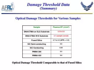
Damage Threshold Data (Summary). Optical Damage Thresholds for Various Samples. Optical Damage Threshold Comparable to that of Fused Silica. Thermal Conductivity . Large Thermal Conductivity 0.12 W/ mK for PMMA [1] 0.82 W/ mK DNA (~7X > PMMA) 0.62 W/ mK DNA-CTMA (~5X > PMMA). [2].

Damage Threshold Data (Summary)
E N D
Presentation Transcript
Damage Threshold Data (Summary) Optical Damage Thresholds for Various Samples Optical Damage Threshold Comparable to that of Fused Silica
Thermal Conductivity • Large Thermal Conductivity • 0.12 W/mK for PMMA[1] • 0.82 W/mK DNA (~7X > PMMA) • 0.62 W/mK DNA-CTMA (~5X > PMMA) [2] DNA & DNA/CTMA [measured - AFRL] PMMA [1] Potential For Getting Heat Out [1] Takashi Kodama, et al., “Heat Conduction through a DNA-Gold Composite,” Nano Letters, 9, 2005 (2009) [2] Hartnett, Cho, Greene and Bar-Cohen, Advances In Heat Transfer, Volume 39, p. 174, Academic Press, 2006 IPITEK
DNA Biopolymer-Based White Solid State Lighting Materials • Ce3+:YAG Phosphor: • Merck: Isiphor YGA 588100 (LED phosphor) • Epoxy: • Epoxy Technology: EPO-TEK OG142-112 (LED epoxy) • DNA-Biopolymer: • 12 wt% DNA-CTMA-C4H9OH • (500 KDa, soxhlet rinse - no dialysis) • DNA – Ogata Research Laboratory • CTMA – Sigma Aldrich (25 wt% CTMA in solution) • C4H9OH – Sigma Aldrich
DNA Biopolymer-Based White Solid State Lighting Processing • 33 wt% Ce3+:YAG-DNA/CTMA • 45 µl drop onto nylon cap • bake @ 40oC for 60 min • (no UV curing required) • 33 wt% Ce3+:YAG-Epoxy • 45 µl drop onto nylon cap • UV cure 100 mW for 10 min • bake @ 40oC for 60 min
DNA Biopolymer-Based White Solid State Lighting Characterization Phosphor + Host Light Source: Photon Micro Light (λ= 470 nm) Sony 100 Camera Speed: 1/160 second Aperture: F5.6 33 wt% Ce3+:YAG-Epoxy 33 wt% Ce3+:YAG-DNA/CTMA
DNA Biopolymer-Based White Solid State Lighting 33 wt% Ce3+:YAG-Epoxy 33 wt% Ce3+:YAG-DNA/CTMA Central Bright Region 6X Larger for DNA-Based Material (6X Brighter ?) Sony 100 Camera Speed: 1/160 second Aperture: F5.6 IGOR PRO Photon Micro Light (λ= 470 nm) 33 wt% Ce3+:YAG-DNA/CTMA 33 wt% Ce3+:YAG-Epoxy iPhotoLux app for Apple iPod Touch J. Grote, “Light emitting diode with a deoxyribonucleic acid (DNA) biopolymer”, US Patent 8,093,802 B1, Jan. 10, 2012
DNA Biopolymer-Based White Solid State Lighting Blue LED 33 wt% Ce3+:YAG-Epoxy 33 wt% Ce3+:YAG-DNA/CTMA More Blue Component with Epoxy-Based Host More Longer Wavelength Components with DNA-Based Host
DNA Biopolymer-Based White Solid State Lighting Chromaticity (CIE 1931 [x, y] Gamut Chart) 33 wt% Ce3+:YAG-DNA/CTMA [0.2441, 0.2877] Exact White [0.3127, 0.3290] 33 wt% Ce3+:YAG-Epoxy [0.1975, 0.2177]
DNA Biopolymer-Based White Solid State Lighting Heat Exposure Epoxy - 66.11 µm thick (flow coat) DNA/CTMA - 59.33 µm thick (flow coat)
DNA Biopolymer-Based White Solid State Lighting 24 Hour UV Exposure (λ = 365 nm) DNA-CTMA Epoxy - 66.11 µm thick (flow coat) DNA/CTMA - 59.33 µm thick (flow coat)
DNA Biopolymer-Based White Solid State Lighting Cost Analysis • Cost Per Gram of Material • DNA/CTMA $6.75 • 0.5g DNA + 4 ml CTMA • (25 wt% solution of CTMA in H2O) • 12 wt% DNA/CTMA in C4H9OH $0.86 (~4X more) • EPO-TEK OG142-112 Epoxy $0.20 • Future DNA materials (estimated 10X-100X cost reduction) • 12 wt% DNA/CTMA in C4H9OH $0.16 (~1.25X less) • $0.06 (~3X less) Phosphor Coating Accounts for 5% - 10% of Cost of White LED
Spin Deposit Vacuum Deposit Cast Ink Jet Print Pulsed Laser Flow Coat Deposition Techniques That Can Be Used Spray Deposit Electro-Spin
Phosphor-DNA/CTMA Phosphor-DNA/CTMA Enhanced Fluorescence in Electrospun Dye-Doped DNA Nanofibers DNA-CTMA-Hemi22 Nanofiber ~10X Film Fluorescent Dye Hemi22 λex= 460 nm (Hemi22) 4-[4-dimethylaminostyryl]- 1-docosylpyridinium bromide Normalized Fluorescence SampleIntensity PMMA Film 2.2 x10⁶ PMMA Nanofiber 1.1 x 10⁷ DNA–CTMA Film 3.9 x 10⁷ DNA–CTMA Nanofiber 2.3 x 10⁸ Acceptor Dye Increased Surface Area Y. Ner, et. al., “Enhanced Fluorescence in Electrospun Dye-Doped DNA Nanofibers ", Soft Matter, 4, 1-7, (2008)
Summary & Conclusions (DNA-CTMA Host vs Epoxy) • Brighter (Higher Efficiency ?) • Closer to Exact White Light (More Longer Wavelengths Present) • Higher UV & Comparable Heat Tolerance (Longer Lifetime ?) • Lower Optical Loss • Acceptable Temperature Stability • Higher Thermal Conductivity • Higher Optical Damage Threshold • Higher Photochemical Stability • Comparable Low Temperature Processing • No UV Curing Required • Longer Shelf Life • Environmentally Friendly • ~4X More Expensive (Currently) • Potentially ~1.25X-3X Less Expensive (Future) Cost may not be an issue
Acknowledgments • Edison Materials Technology Center (EMTEC) • Air Force Research Laboratory • Materials &Manufacturing Directorate (AFRL/RX) • Merck (Ce3+:YAG phosphor) • Rajesh Naik (jpeg to gamut chart conversion) • Timothy Gorman (IGOR PRO conversion) • Danny Grote (iPhotoLux conversion) • Elizabeth Steenbergen (spectral data) • ID Cast • Wright Brothers Institute

