Radiation Tolerance Evaluation of SiGe HBTs for High-Energy Physics Applications
170 likes | 203 Vues
This study explores the radiation tolerance of SiGe HBT transistors under gamma exposure, crucial for high-energy physics experiments such as ATLAS Upgrade. SiGe technology offers advantages like low noise design and small base resistance, enhancing performance in particle physics. The research includes device sizes, radiation tolerance studies by leading vendors like IBM and IHP, as well as experimental results on current gain and specific mechanisms for device degradation. The investigation involves gamma, neutron, and proton irradiations with over 22,000 measurements planned to understand transistor behavior under different conditions thoroughly.

Radiation Tolerance Evaluation of SiGe HBTs for High-Energy Physics Applications
E N D
Presentation Transcript
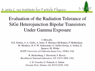
SCIPP SCIPP Santa Cruz Institute for Particle Physics Evaluation of the Radiation Tolerance of SiGe Heterojunction Bipolar Transistors Under Gamma Exposure J. Metcalfe, D.E. Dorfan, A. A. Grillo, A. Jones, F. Martinez-McKinney, P. Mekhedjian, M. Mendoza, H. F.-W. Sadrozinski, G. Saffier-Ewing, A. Seiden, E. Spencer, M. Wilder SCIPP, University of California Santa Cruz, 95064, USA R. Hackenburg, J. Kierstead, S. Rescia Brookhaven National Laboratory, NY 11973-5000, USA J. D. Cressler, G. Prakash, A. Sutton Georgia Tech, Atlanta, GA 30332-0250, USA
SCIPP SCIPP Power Constraints ATLAS already has over 4,000 heavy copper cables for the SCT alone! -> Need to reduce power consumption w/out sacrificing noise performance at high radiation levels for ATLAS Upgrade if we want to replace the TRT with silicon. Target for Front-End Channel (Analog Section Only): Current ATLAS: <400mW @ 15pF (long strips at outer radius, 60cm) 2 mW <160mW @ 6pF (short strips at mid-radius, 20 cm) Rad Tolerance of SiGe HBT Jessica Metcalfe
SCIPP SCIPP Why SiGe? • Advantages of SiGe Bipolar Over CMOS for Silicon Strip Detectors • A key element in the design of low noise, fast shaping, charge amplifiers is high transconductance in the first stage. • With CMOS technologies, this requires relatively larger bias currents than with bipolar technologies. • The changes that make SiGe Bipolar technology operate at 100 GHz for the wireless industry coincide with the features that enhance performance in high energy particle physics applications. • Small feature size increases radiation tolerance. • Extremely small base resistance (of order 10-100 W) affords low noise designs at very low bias currents. • These design features are important for applications with: • Large capacitive loads (e.g. 5-15 pF silicon strip detectors) • Fast shaping times (e.g. accelerator experiments with beam crossing times of tens of nanoseconds in order to identify individual beam crossing events) Rad Tolerance of SiGe HBT Jessica Metcalfe
SCIPP SCIPP SiGe Technology • Origin of radiation tolerance: • Small active volume of the transistor • Thin emitter-base spacer oxide (weakest spot) • SiGe Technology Readily Available • Over 25 foundries • Some Vendors: IBM, IHP, JAZZ, Motorola, STm… • IBM offers 3 generations (4th on the way): • 5HP (5AM): 0.5x1 -> 0.5x20 mm2 • 7HP: 0.2x1 -> 0.28x20 mm2 • 8HP: 0.12x0.52 -> 0.12x8 mm2 • IHP SiGe Technology: • Radiation Tolerance Study by: • Miguel Ullán, et al CNM, Barcelona • Ned Spencer (SCIPP) has designed an amplifier with IHP as a proof of principle Rad Tolerance of SiGe HBT Jessica Metcalfe
Device Sizes: 0.5x1 mm2 0.5x2.5 mm2 0.5x10 mm2 0.5x20 mm2 4x5 mm2 ATLAS Upgrade Outer Radius Pre-rad SCIPP SCIPP 4.15 x 10¹³ 1.15 x 10¹⁴ 3.50 x 10¹⁴ Mid Radius Inner Radius 1.34 x 10¹⁵ 3.58 x 10¹⁵ 1.05 x 10¹⁶ Summary of 2004 Proton Results • Irradiation Procedure: • 5AM devices were sent to CERN and exposed to a 24GeV proton source with the highest fluence taking 5 days to accumulate. • The leads were grounded during irradiation --> worst case scenario. • The transistors were annealed to improve performance. • Special thanks to the RD50 collaboration, especially, Michael Moll and Maurice Glaser!! Rad Tolerance of SiGe HBT Jessica Metcalfe
Current Gain, b, vs. Ic for 0.5x10 mm2 Pre-rad and for All Fluences Including Full Annealing SCIPP SCIPP Current Gain, b Ic [A] Summary of 2004 Proton Results • Conclusions: • @ 3x10¹⁴, Ic low enough for substantial power savings over CMOS • @1x10¹⁵, Ic good for a front transistor (uses a higher current while minimizing noise) Before Irradiation Increasing Fluence Lowest Fluence Current Gain, b Highest Fluence Rad Tolerance of SiGe HBT Jessica Metcalfe
SCIPP SCIPP Current Investigation Gamma, Neutron & Proton Irradiations: • Over 22,000 measurements planned!!! • Developed an automatic measuring system at SCIPP and BNL • ->Plug in a chip, take all measurements for all transistors at once • Will this be enough to understand the specific mechanisms for device degradation?? • Tests: • 8HP HBT • 8HP HBT--Biased • For gammas & protons • 8HP HBT--Shield • For gammas & neutrons • 7HP HBT • 5AM HBT • 8HP Resistor • 8HP Capacitor • Measurements: • Forward Gummel • Vcb=0V, 0.5V • Inverse Gummel • Vcb=0V, 0.5V • Early Voltage • Neutral Base Recombination • M-1, Avalanche Factor • Resistance • Capacitance • Runs: • Characterization (Pre-Rad) • Post-Rad (No Anneal) • Anneal 1 (5 days @ 25C) • Anneal 2 (1 day @ 60C) • Anneal 3 (1 day @ 100C) • Anneal 4 (6 days @ 100C) Rad Tolerance of SiGe HBT Jessica Metcalfe
SCIPP SCIPP Current Investigation Characterization measurements: • Irrad Procedure for Gammas: • 60Co source at BNL • Measurements performed at BNL • Total dose of 100 Mrads • Devices tested at steps: • 500 kRad • 1 Mrad • 5 Mrad • 10 Mrad • 50 Mrad • 100 Mrad • Devices shorted during irrad • Except one 8HP HBT chip biased • No Shield* (next round) Rad Tolerance of SiGe HBT Jessica Metcalfe
SCIPP SCIPP Preliminary Gamma Results The damage caused by gammas and protons for comparable doses/fluences is very similar even though starting gain values are different. This may imply that most of the gain degradation is induced by ionization damage. Rad Tolerance of SiGe HBT Jessica Metcalfe
SCIPP SCIPP Preliminary Gamma Results • 8HP has the best overall performance. • The damage mechanism in the 7HP is distinctly different due to structural differences. • “ Ionizing radiation has been shown to damage the EB spacer region in these SiGe HBTs, and produce a perimeter-dependent space-charge generation/recombination (G/R) base-current leakage component that progressively degrades the base current (and current gain) as the fluence increases. …the 7HP device degrades much more rapidly than the 5HP device. This result is consistent with significantly higher EB electric field under the EB spacer region in the 7HP device, which has both more abrupt doping profiles…as well as a decreased EB spacer thickness compared to the 5HP device…” Silicon-Germanium Heterojunction Bipolar Transistors, Cressler, Niu Rad Tolerance of SiGe HBT Jessica Metcalfe
SCIPP SCIPP Preliminary Gamma Results The gain of the biased 8HP HBT performs much better after 100 MRads, even though it started at a lower gain value!! The gain of the shorted 8HP HBT degrades more rapidly after 100 MRads. The gain for the biased transistor started at a lower gain value (normal fluctuation in starting gain), but by 5 MRads showed less radiation damage. At higher doses this effect becomes enhanced indicating that device performance at high doses for transistors shorted during irradiation will be improved. Rad Tolerance of SiGe HBT Jessica Metcalfe
SCIPP SCIPP Preliminary Gamma Results: Biased Before Irradiation Highest Dose, 100 MRad Biased during irradiation Lowest Dose, 500 kRad Transistor performance at for 8HP at 100 Mrad is very good--the current gain is still 77 at 1mA!! (No annealing yet!) Rad Tolerance of SiGe HBT Jessica Metcalfe
SCIPP SCIPP Preliminary Gamma Results Universal behavior is independent of transistor geometry when compared at the same current density Jc and for similarly shorted or biased transistors. For a given current density D(1/b) scales linearly with the log of the fluence. This precise relation allows the gain after irradiation to be predicted for other SiGe HBTs for shorted devices before annealing. Hence, the operating currents can be scaled to desired device sizes for Front-End Channel simulations. Rad Tolerance of SiGe HBT Jessica Metcalfe
SCIPP SCIPP Preliminary Gamma Results Qualifications for a good transistor: A gain of 50 is a good figure of merit for a transistor to use in a front-end circuit design. Requires only 0.28 mA to reach a gain of 50!! At 100 Mrad (before annealing!), the dose reached at the mid-region of ATLAS Upgrade, very small currents can be used in the design of the front transistor and the others in a Front-End Channel design. This provides flexibility in choosing the operating current for the transistor, which allows the FEC design to optimize other factors such as matching. Rad Tolerance of SiGe HBT Jessica Metcalfe
SCIPP SCIPP Preliminary Power Savings Pre-Amp Amplifier-Shaper Comparator Total 0.25 mm 300 mA 210 mA 120 mA 1.5 mW CMOS (120 mA)* (1.1 mW)* SiGe 150 mA 13 mA 16.6 mA 0.36 mW IHP (40 mA)* (0.14 mW)* * Low capacitance (7 pF) = Short strip FEE Design 360 mW/Channel SPICE simulations with IHP models predicts these currents yield a Front-End Channel design using only 360 mW!! Current ATLAS uses 2 mW! *CMOS numbers courtesy of Kaplon Rad Tolerance of SiGe HBT Jessica Metcalfe
SCIPP SCIPP Conclusions • Radiation damage may be primarily due to ionization damage. • 8HP appears to be more Rad Tolerant than 5AM or 7HP. • HBTs biased during irradiation (closer to actual conditions in ATLAS) show less damage--interesting to see after annealing. • Preliminary results of gamma irradiations indicate that IBM 8HP SiGe Technology is sufficiently Rad Tolerant for ATLAS Upgrade SCT application. (Irradiations already underway will verify this.) • May be able to reduce power by 75% from 1500 mW to 360 mW! Rad Tolerance of SiGe HBT Jessica Metcalfe