Download

1 / 21
270 likes | 633 Vues
Explore the intricate Memory Hierarchy in computer systems, from Cache Memory to Auxiliary Memory, with detailed examples and diagrams. Learn about Main Memory Organization and Cache Design Elements for optimal performance.

E N D
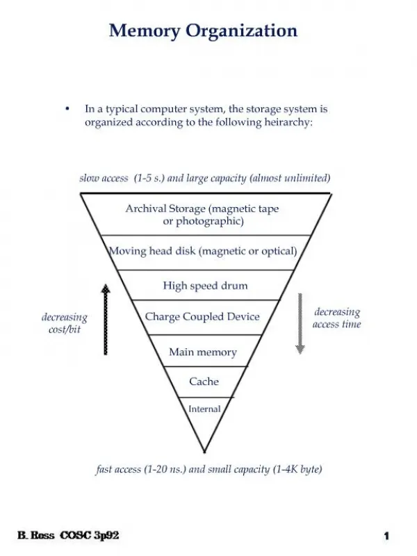
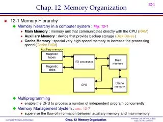
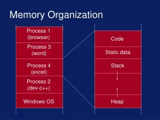
Chap. 12 Memory Organization • 12-1 Memory Hierarchy • Memory hierarchy in a computer system : Fig. 12-1 • Main Memory : memory unit that communicates directly with the CPU (RAM) • Auxiliary Memory : device that provide backup storage (Disk Drives) • Cache Memory : special very-high-speed memory to increase the processing speed (Cache RAM) • Multiprogramming • enable the CPU to process a number of independent program concurrently • Memory Management System : sec. 12-7 • supervise the flow of information between auxiliary memory and main memory
12-2 Main Memory • Bootstrap Loader • A program whose function is to start the computer software operating when power is turned on • RAM and ROM Chips • Typical RAM chip : Fig. 12-2 • 128 X 8 RAM : 27 = 128 (7 bit address lines) • Typical ROM chip : Fig. 12-3 • 512 X 8 ROM : 29 = 512 (9 bit address lines) Bootstrap Loader Bootstrap ROM Boot ROM
Memory Address Map • Memory Configuration : 512 bytes RAM + 512 bytes ROM • 1 x 512 byte ROM + 4 x 128 bytes RAM • Memory Address Map : Tab. 12-1 • Address line 9 8 • RAM 1 0 0 : 0000 - 007F • RAM 1 0 1 : 0080 - 00FF • RAM 1 1 0 : 0100 - 017F • RAM 1 1 1 : 0180 - 01FF • Address line 10 • ROM 1 : 0200 - 03FF • Memory Connection to CPU : Fig. 12-4 • 2 x 4 Decoder : RAM select (CS1) • Address line 10 • RAM select : CS2 • ROM select : CS2의 Invert • 참고 • RD : ROM 의 CS1은 보통 OE(Output Enable)로 사용
12-3 Auxiliary Memory • Magnetic Disk : Fig. 12-5,FDD, HDD • Magnetic Tape : Backup or Program 저장 • Optical Disk : CDR, ODD, DVD • 12-4 Associative Memory • Content Addressable Memory (CAM) • A memory unit accessed by content • Block Diagram : Fig. 12-6 이름 주소 A Register 101 111100 K Register 111 000000 Word 1 100 111100 M = 0 Word 2 101000011 M=1 Argument Key (Mask) Memory 내용 Match Logic M = 1 일때 출력
m word x n cells per word : Fig. 12-7 • Match Logic • One cell of associative memory : Fig. 12-8 • Input = 1 or 0 에 따라 Write 신호와 동시에 F/F에 저장 • A 와 K 에 의해 Match Logic 에서 M=1 이면 (M을 READ에 직접 연결 가능함) • Read 신호에 따라 F/F에서 데이터를 읽는다
Match Logic : Fig. 12-9 • Aj = Argument, Fij = Cell ij 번째 bit • j 번째 1 bit match 조건 xj = Aj Fij (1 AND 1)+ Aj’ Fij’ (0 AND 0) • 1 - n 까지 n bits match 조건 Mi = x1x2…..xn • Key bit Kj : xj + Kj’ • Kj = 0 : Aj와 Fij는 no comparison ( Kj : xj + 1 = 1 ) • Kj = 1 : Aj와 Fij는 comparison ( Kj : xj + 0 = xj ) • Match Logic for word I : Mi = (x1 + K1’) (x2 + K2’)…. (xn + Kn’) = (xj + Kj’) = (Aj Fij + Aj’ Fij’ + Kj’)
12-5 Cache Memory • Locality of Reference • the references to memory tend to be confined within a few localized areas in memory • Cache Memory : a fast small memory • keeping the most frequently accessed instructions and data in the fast cache memory • Cache 의 설계 요소 • cache size : 보통 256 K byte (최대 512 K byte) • mapping method : 1) associative, 2) direct, 3) set-associative • replace algorithm : 1) LRU, 2) LFU, 3) FIFO • write policy : 1) write-through, 2) write-back • Hit Ratio • the ratio of the number of hits divided by the total CPU references (hits + misses) to memory • hit : the CPU finds the word in the cache (보통 0.9 이상) • miss : the word is not found in cache (CPU must read main memory) • 예제 : cache memory access time = 100 ns, main memory access time = 1000 ns, hit ratio = 0.9 • 1 회 miss : 1 x 1000 ns • 9 회 hit : 9 x 100 ns 총 10 회 Memory 참조 Cache가 없으면 1000 ns, 따라서 약 5 배 성능 향상 1900 ns / 10 회 = 190ns
Mapping • The transformation of data from main memory to cache memory • 1) Associative mapping • 2) Direct mapping • 3) Set-associative mapping • Example of cache memory : Fig. 12-10 main memory : 32 K x 12 bit word (15 bit address lines) cache memory : 512 x 12 bit word • CPU sends a 15-bit address to cache • Hit : CPU accepts the 12-bit data from cache • Miss : CPU reads the data from main memory (then data is written to cache) • Associative mapping : Fig. 12-11 • Cache memory로 고가의 associative memory 사용 • Address 와 Data 가 직접 Cache memory에 사용됨 • Direct mapping : Fig. 12-12 • Cache memory로 저가의 일반 memory 사용 • Tag field (n - k) 와 Index field (k)를 사용 • 2k words cache memory +2n words main memory • Tag = 6 bit (15 - 9), Index = 9 bit Cache Coherence (Sec. 13-5)
Direct mapping cache organization : Fig. 12-13 • 예제 : 02000번지를 읽는 경우 • 1) 우선 Index 000을 cache 에서 찾는다 • 2) 다음은 Tag를 cache에서 비교한다 • 3) 000Index에 있는 cachetag는 00 이다 (02가 아니다) • 4) 따라서 miss • 5) 그러므로 main memory에서 data read (address 02000 = 5670 read) Tag (6 bit) 00 - 63 Index (9 bit) 000 - 511
Direct mapping cache with block size of 8 words : Fig. 12-14 • 64 block x 8 word = 512 cache words size • 8 word 를 1개의 block 단위로 update • Set-associative mapping : Fig. 12-15 (two-way) • Direct mapping ( Fig. 12-13(b))에서 같은 Index에 다른 tag를 자주 읽으면 속도가 저하됨 ( 예제 02777, 01777 ) • 따라서 set의 개수를 증가시키면 속도가 향상된다.
Replacement Algorithm : cache miss or full 일때 • 1) LRU (Least Recently Used) : 최근에 가장 적게 사용된 block 교체 • 2) LFU (Least Frequently Used) : 사용 빈도가 가장 적은 block 교체 • 3) FIFO (First-In First-Out) : 가장 오래된 block 교체 • Writing to Cache : Cache Coherence(Sec. 13-5) • Cache에 있는 내용이 변경된(WRITE) 경우, Cache의 block이 교체되기 전에 main memory에 내용도 update 해야 함 • 1) Write-through : Cache write 와 동시에 main memory도 항상 동시에 write 한다. • 2) Write-back : Cache write 시에 내용이 변경되었다는 flag 만 set해 놓고 나중에 block이 교체되기 전에 flag를 검사하여 변경된 부분만 나중에 write 한다. • 따라서 Write-back 방식은 main memory가 무효한 상태에 빠져 있을 수 있다. • Cache Initialization • Cache is initialized : 이때 cache 는 empty 상태이고 invalid data를 갖을 수 있다. • 1) when power is applied to the computer • 2) when main memory is loaded with a complete set of programs from auxiliary memory • valid bit • indicate whether or not the word contains valid data Cache READ는 문제 없음 Main memory 와 Cache memory의 내용이 동일해야 함 : 통일성(일관성) 유지
12-6 Virtual Memory • Virtual Memory : Auxiliary memory Main memory • Translate program-generated (Aux. Memory) address into main memory location • Give programmers the illusion that they have a very large memory, even though the computer actually has a relatively small main memory • 예제 : Intel Pentium Processor • Physical Address Lines = A0 - A31 : 232 = 230 X 22 = 4 Giga • Logical Address = 46 bits address : 246 = 240 X 26 = 64 Tera • Address Space & Memory Space • Address Space : Virtual Address • Address used by a programmer • Memory Space : Physical Address(Location) • Address in main memory • 예제 : Fig. 12-16 • address space (N) = 1024 K = 220 • Auxiliary Memory • memory space (M) = 32 K = 215 • main Memory
Memory table for mapping a virtual address : Fig. 12-17 • Translate the 20 bits Virtual address into the 15 bits Physical address • Address Mapping Using Pages : Fig. 12-18 • Address mapping 을 간단하게 하기 위하여 사용 • Address space와 memory space를 fixed size로 분할하여 사용함 • Address space : 1 K page 로 분할 • Memory space : 1 k block으로 분할 • Address space의 4 개 page가 memory space에 block에 들어 갈수 있다.
Associative memory page table : Fig. 12-20 • Associative memory를 이용하여 block number(01)를 곧바로 찾는다 • Page(Block) Replacement • Page Fault : the page referenced by the CPU is not in main memory • a new page should be transferred from auxiliary memory to main memory • Replacement algorithm : FIFO 와 LRU 주로 사용
12-7 Memory Management Hardware • Basic components of a Memory Management Unit • 1) Address mapping • 2) Common program sharing • 3) Program protection • MMU : OS 에서 지원 해야 함 • 1) CPU에 내장된 형태 • 2) 별도의 memory controller 형태 • Segment • A set of logically related instruction or data elements associated with a given name • 예제 : a subroutine, an array of data, a table of symbol, user’s program • Logical Address • the address generated by a segmented program • similar to virtual address • Virtual Address : fixed-length page • Logical Address : variable-length segment
Segmented-page MMU • Fig. 12-21(a) : 2 개의 table(segment, page)을 사용함 • 따라서 2 개의 table을 읽는데 많은 시간이 소모됨 • Fig. 12-21(b) : Associative memory를 이용한 1 개의 table을 사용함 • 따라서 속도가 빠르다 • TLB (Translation Look-a-side Buffer) • associative memory를 이용한 most recently reference table • Numerical Example • 예제 : Logical address & Physical address (Fig. 12-22) • Logical Address : • 4 bit segment : 16 segments • 8 bit page : 256 pages • 8 bit word : 256 address field • Physical Address : • 12 bit block : 4096 blocks • 8 bit word : 256 address field Address or Index
예제 : Logical & Physical address assignment (Fig. 12-23) Logical Address Page Table Segment Page Word Block number 019 를 찾는다
Memory Protection • Typical segment descriptor : Fig. 12-25 • Access Rights : protecting the programs residing in memory • 1) Full read and write privileges : no protection • 2) Read only : write protection • 3) Execute only : program protection • 4) System only : operating system protection segment Length Base address