Understanding Memory Organization: Hierarchy, Types, and Management in Computing
This article delves into the essential concepts of memory organization in computer systems, focusing on the memory hierarchy. It examines different types of memory, including main memory (RAM and ROM), auxiliary memory, cache memory, and associative memory. The article explains how these memory types interact with the CPU, the significance of memory management, and the impact of the memory hierarchy on access speed and cost. Key concepts such as cache mapping, hit ratios, and address mapping are also discussed to provide a comprehensive understanding of effective memory organization.

Understanding Memory Organization: Hierarchy, Types, and Management in Computing
E N D
Presentation Transcript
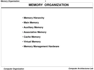
MEMORY ORGANIZATION • Memory Hierarchy • Main Memory • Auxiliary Memory • Associative Memory • Cache Memory • Virtual Memory • Memory Management Hardware
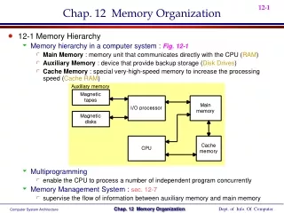
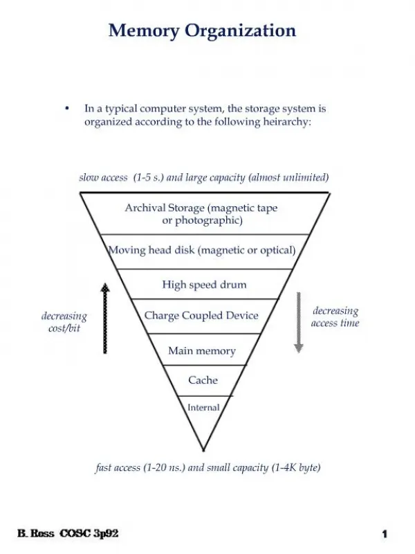
Memory Hierarchy MEMORY HIERARCHY Memory Hierarchy is to obtain the highest possible access speed while minimizing the total cost of the memory system Auxiliary memory Magnetic I/O Main tapes memory processor Magnetic disks Cache CPU memory Register Cache Main Memory Magnetic Disk Magnetic Tape
Main Memory MAIN MEMORY RAM and ROM Chips Typical RAM chip Chip select 1 CS1 Chip select 2 CS2 128 x 8 Read RD 8-bit data bus RAM Write WR 7-bit address AD 7 Memory function State of data bus CS1 CS2 RD WR Inhibit High-impedence 0 0 x x Inhibit High-impedence 0 1 x x Inhibit High-impedence 1 0 0 0 Write Input data to RAM 1 0 0 1 Output data from RAM Read 1 0 1 x Inhibit High-impedence 1 1 x x Typical ROM chip CS1 Chip select 1 CS2 Chip select 2 512 x 8 8-bit data bus ROM 9-bit address AD 9
Main Memory Address bus Hexa address Component 10 9 8 7 6 5 4 3 2 1 RAM 1 RAM 2 RAM 3 RAM 4 ROM 0000 - 007F 0080 - 00FF 0100 - 017F 0180 - 01FF 0200 - 03FF 0 0 0 x x x x x x x 0 0 1 x x x x x x x 0 1 0 x x x x x x x 0 1 1 x x x x x x x 1 x x x x x x x x x Memory Connection to CPU - RAM and ROM chips are connected to a CPU through the data and address buses - The low-order lines in the address bus select the byte within the chips and other lines in the address bus select a particular chip through its chip select inputs MEMORY ADDRESS MAP Address space assignment to each memory chip Example: 512 bytes RAM and 512 bytes ROM
Main Memory CONNECTION OF MEMORY TO CPU CPU Address bus 16-11 10 9 8 7-1 RD WR Data bus Decoder 3 2 1 0 CS1 CS2 128 x 8 Data RD RAM 1 WR AD7 CS1 CS2 128 x 8 Data RD RAM 2 WR AD7 CS1 CS2 128 x 8 Data RD RAM 3 WR AD7 CS1 CS2 128 x 8 Data RD RAM 4 WR AD7 CS1 CS2 1- 7 512 x 8 Data 8 ROM AD9 9
Auxiliary Memory file i block 1 block 2 EOF block 3 R1 R2 R3 R4 R5 R6 block 3 IRG R1 EOF R3 R2 block 1 R5 R4 block 2 Moving Head Disk Fixed Head Disk Track AUXILIARY MEMORY Information Organization on Magnetic Tapes Organization of Disk Hardware
Associative Memory ASSOCIATIVE MEMORY - Accessed by the content of the data rather than by an address - Also called Content Addressable Memory (CAM) Hardware Organization Argument register(A) Key register (K) Match register Input Associative memory array and logic M Read m words Write n bits per word - Compare each word in CAM in parallel with the content of A(Argument Register) - If CAM Word[i] = A, M(i) = 1 - Read sequentially accessing CAM for CAM Word(i) for M(i) = 1 - K(Key Register) provides a mask for choosing a particular field or key in the argument in A (only those bits in the argument that have 1’s in their corresponding position of K are compared)
Associative Memory ORGANIZATION OF CAM Aj A1 An Kj K1 Kn C1j C1n M1 C11 Word 1 Cij Cin Word i Ci1 Mi Cmj Cmn Word m Cm1 Mm Bit j Bit n Bit 1 Internal organization of a typical cell Cij Aj Kj Input Write R S Match To M F ij i logic Read Output
Associative Memory MATCH LOGIC K A K A K A 1 1 2 2 n n F' F F' F F . . . . F' i1 in in i1 i2 i2 M i
Cache Memory CACHE MEMORY The references to memory at any given time interval of time tend to be confined within a few localized areas in memory. This phenomenon is known as the property of locality of reference. If the active portions of the program and data are placed in a fast small memory, the average memory access time can be reduced, thus reducing the total execute on time of the program. Such a fast small memory is referred to as a cache memory. The performance of cache memory is frequently measured in terms of a quantity called hit ratio. When the CPU refers to memory and finds the word in cache, it is said to produce a hit. If the word is not found in cache, it is in main memory and it counts as a miss. The ratio of the number of hits divided by the total CPU references to memory is the hit ratio. Main memory CPU Cache memory
Cache Memory MEMORY AND CACHE MAPPING - ASSOCIATIVE MAPPLING - Mapping Function The transformation of data from main memory to cache memory is Referred to as a mapping process. Associative mapping Direct mapping Set-associative mapping Associative Mapping -The associative memory stores both the address and content Of the memory word. address (15 bits) Argument register Address Data 0 1 0 0 0 3 4 5 0 CAM 0 2 7 7 7 6 7 1 0 2 2 2 3 5 1 2 3 4
Cache Memory MEMORY AND CACHE MAPPING - DIRECT MAPPING - - Each memory block has only one place to load in Cache - Mapping Table is made of RAM instead of CAM - n-bit memory address consists of 2 parts; k bits of Index field and n-k bits of Tag field - n-bit addresses are used to access main memory and k-bit Index is used to access the Cache Addressing Relationships Tag(6) Index(9) 00 000 32K x 12 000 512 x 12 Main memory Cache memory Address = 15 bits Address = 9 bits Data = 12 bits Data = 12 bits 777 77 777 Direct Mapping Cache Organization Memory Memory data address Cache memory 00000 1 2 2 0 Index Tag Data address 0 0 1 2 2 0 00777 2 3 4 0 000 01000 3 4 5 0 01777 4 5 6 0 02000 5 6 7 0 0 2 6 7 1 0 777 02777 6 7 1 0
Cache Memory DIRECT MAPPING Operation - CPU generates a memory request with (TAG;INDEX) - Access Cache using INDEX ; (tag; data) Compare TAG and tag - If matches -> Hit Provide Cache[INDEX](data) to CPU - If not match -> Miss M[tag;INDEX] <- Cache[INDEX](data) Cache[INDEX] <- (TAG;M[TAG; INDEX]) CPU <- Cache[INDEX](data) Direct Mapping with block size of 8 words Index tag data 6 6 3 Tag Block Word 000 0 1 3 4 5 0 Block 0 0 1 007 6 5 7 8 INDEX 010 Block 1 017 0 2 770 Block 63 777 0 2 6 7 1 0
Cache Memory Index Tag Data Tag Data 000 0 1 3 4 5 0 0 2 5 6 7 0 777 0 2 6 7 1 0 0 0 2 3 4 0 MEMORY AND CACHE MAPPING - SET ASSOCIATIVE MAPPING - - Each memory block has a set of locations in the Cache to load Set Associative Mapping Cache with set size of two Operation - CPU generates a memory address(TAG; INDEX) - Access Cache with INDEX, (Cache word = (tag 0, data 0); (tag 1, data 1)) - Compare TAG and tag 0 and then tag 1 - If tag i = TAG -> Hit, CPU <- data i - If tag i TAG -> Miss, Replace either (tag 0, data 0) or (tag 1, data 1), Assume (tag 0, data 0) is selected for replacement, (Why (tag 0, data 0) instead of (tag 1, data 1) ?) M[tag 0, INDEX] <- Cache[INDEX](data 0) Cache[INDEX](tag 0, data 0) <- (TAG, M[TAG,INDEX]), CPU <- Cache[INDEX](data 0)
Cache Memory CACHE WRITE Write Through When writing into memory If Hit, both Cache and memory is written in parallel If Miss, Memory is written For a read miss, missing block may be overloaded onto a cache block Write-Back (Copy-Back) When writing into memory If Hit, only Cache is written If Miss, missing block is brought to Cache and write into Cache For a read miss, candidate block must be written back to the memory
Virtual Memory address space memory space Mapping virtual address (logical address) physical address address generated by programs actual main memory address VIRTUAL MEMORY Give the programmer the illusion that the system has a very large memory, even though the computer actually has a relatively small main memory Address Space(Logical) and Memory Space(Physical) Address Mapping Memory Mapping Table for Virtual Address -> Physical Address Virtual address Main memory Virtual Memory Main address address mapping memory register register table Physical Address Memory table Main memory buffer register buffer register
Virtual Memory PAGE REPLACEMENT Decision on which page to displace to make room for an incoming page when no free frame is available Modified page fault service routine • 1. Find the location of the desired page on the backing store • 2. Find a free frame • - If there is a free frame, use it • - Otherwise, use a page-replacement algorithm to select a victim frame • - Write the victim page to the backing store • 3. Read the desired page into the (newly) free frame • 4. Restart the user process valid/ invalid bit frame swap out victim 1 page 2 change to victim 0 i v f invalid 3 4 swap v f reset page desired table for page in new page backing store page table physical memory
Virtual Memory PAGE REPLACEMENT ALGORITHMS FIFO Reference string 7 0 1 2 0 3 0 4 2 3 0 3 2 1 2 0 1 7 0 1 2 7 7 2 2 4 4 0 0 7 7 7 7 4 0 0 0 0 3 3 3 2 2 2 1 1 1 0 0 1 1 1 0 0 0 3 3 3 2 2 2 1 Page frames FIFO algorithm selects the page that has been in memory the longest time Using a queue - every time a page is loaded, its identification is inserted in the queue Easy to implement May result in a frequent page fault - Optimal Replacement (OPT) - Lowest page fault rate of all algorithms Replace that page which will not be used for the longest period of time Reference string 7 0 1 2 0 3 0 4 2 3 0 3 2 1 2 0 1 7 0 1 2 7 7 7 2 2 2 7 2 4 0 0 0 0 0 0 0 1 1 1 3 1 3 3 Page frames
Virtual Memory PAGE REPLACEMENT ALGORITHMS LRU - OPT is difficult to implement since it requires future knowledge - LRU uses the recent past as an approximation of near future. Replace that page which has not been used for the longest period of time Reference string 7 0 1 2 0 3 0 4 2 3 0 3 2 1 2 0 1 7 0 1 4 7 7 2 4 4 1 2 7 0 1 1 0 0 0 0 0 0 3 3 3 0 0 2 1 1 3 3 2 2 2 2 7 Page frames - LRU may require substantial hardware assistance - The problem is to determine an order for the frames defined by the time of last use
Memory Management Hardware MEMORY MANAGEMENT HARDWARE Basic Functions of MM - Dynamic Storage Relocation - mapping logical memory references to physical memory references - Provision for Sharing common information stored in memory by different users - Protection of information against unauthorized access Segmentation - A segment is a set of logically related instructions or data elements associated with a given name - Variable size User's view of memory • The user does not think of • memory as a linear array • of words. Rather the user • prefers to view memory as • a collection of variable • sized segments, with no • necessary ordering among • segments. Stack Subroutine Symbol Table SQRT Main Program User's view of a program
Memory Management Hardware SEGMENTATION - A memory management scheme which supports user's view of memory - A logical address space is a collection of segments - Each segment has a name and a length - Address specify both the segment name and the offset within the segment. - For simplicity of implementations, segments are numbered. Segmentation Hardware Segment Table s limit base CPU (s,d) Memory y < + n error
Memory Management Hardware SEGMENTATION EXAMPLE 1400 Stack Subroutine Segment 0 Segment 3 2400 Segment 0 Symbol 3200 Table Segment 4 SQRT Segment 3 Main Segment 1 4300 Program Segment 2 4700 Segment 2 Segment 4 Logical Address Space 5700 6300 Segment 1 Segment Table 6700 limit base 1000 1400 0 1 400 6300 2 400 4300 3 1100 3200 4 1000 4700
Memory Management Hardware SHARING OF SEGMENTS Editor limit base 43062 0 25286 43062 Segment 0 1 4425 68348 Editor Segment Table Data 1 (User 1) 68348 Data 1 Segment 1 72773 Logical Memory (User 1) 90003 Data 2 98556 limit base Editor 0 25286 43062 1 8550 90003 Physical Memory Segment 0 Segment Table (User 2) Data 2 Segment 1 Logical Memory (User 2)
Memory Management Hardware SEGMENTED PAGE SYSTEM Logical address Segment Page Word Segment table Page table + Block Word Physical address
Memory Management Hardware IMPLEMENTATION OF PAGE AND SEGMENT TABLES Implementation of the Page Table - Hardware registers (if the page table is reasonably small) - Main memory • - Page Table Base Register(PTBR) points to PT • - Two memory accesses are needed to access • a word; one for the page table, one for the word - Cache memory (TLB: Translation Lookaside Buffer) - To speedup the effective memory access time, a special small memory called associative memory, or cache is used Implementation of the Segment Table Similar to the case of the page table
Memory Management Hardware Logical address format: 16 segments of 256 pages each, each page has 256words 4 8 8 Page Word Segment 20 2 x 32 Physical Physical address format: 4096 blocks of 256 words each, each word has 32bits memory 12 8 Word Block Hexa address Page number Page 0 60000 Segment Page Block 60100 Page 1 6 00 012 6 01 000 Page 2 60200 6 02 019 6 03 053 Page 3 6 04 A61 60300 60400 Page 4 604FF (a) Logical address assignment (b) Segment-page versus memory block assignment EXAMPLE Logical and Physical Addresses Logical and Physical Memory Address Assignment
Memory Management Hardware Segment Page Block 6 02 019 6 04 A61 LOGICAL TO PHYSICAL MEMORY MAPPING Segment and page table mapping Logical address (in hexadecimal) 6 02 7E Segment table Page table Physical memory 00 0 00000 Block 0 000FF 6 35 35 012 36 000 01200 37 019 Block 12 38 053 012FF A3 39 F A61 01900 32-bit word 0197E 019FF A3 012 Associative memory mapping
Memory Management Hardware Base address Length Protection MEMORY PROTECTION Protection information can be included in the segment table or segment register of the memory management hardware - Format of a typical segment descriptor - The protection field in a segment descriptor specifies the Access Rights to the particular segment - In a segmented-page organization, each entry in the page table may have its own protection field to describe the Access Rights of each page - Access Rights: Full read and write privileges. Read only (write protection) Execute only (program protection) System only (O.S. Protection)
A Typical Cache and TLB Design From translator CPU Virtual Address Real Address Virtual Address Page Number Line Number Word in Line To translator A CPU Memory Hash Function Real Address Data TLB Cache S S A Real Address Compare Addresses & Select Data Compare Virtual Addresses Data Word Select & Align To Main Memory S = Select Data Out
Structure of Cache Entry and Cache Set Real Address Tag Data Valid Cache Entry Entry 1 Entry 2 Entry E Replacement status Cache Set
Cache Operation Flow Chart Receive Virtual Address Use Line Number to Select Set Hash Page Number Search TLB Read Out Address Tags A yes Compare Addresses In TLB ? no yes Match ? Update Replacement Status in TLB Send Virtual Address to Translator no Send Real Address to Main Memory Update Replacement Status Use Page & Segment tables to Translate Address Select Correct Line Receive Line from Main Memory Store Line in Cache Put in TLB Select Correct Word from Line A Read Out
Virtual Address Format - Example Page number Byte within page Byte within line 31 21 20 17 12 11 10 4 3 2 1 0 Byte within word Select set in cache Select set in TLB Map through page directory Word within line Map through page table Line number Virtual Address of Fairchild Clipper


![[Packet] My Memory Organization](https://cdn1.slideserve.com/1905829/packet-my-memory-organization-dt.jpg)