Front End Circuit.
Front End Circuit. ASIC. -Amit Tawde. CZT FRONT END ELECTRONICS INTERFACE. I/O signal. CZT. ASIC. FRONT END ELECTRONICS. TO PROCESSING ELECTRONICS. +/-15V. -500 V BIAS. +/-2V. FEATURES OF ASIC XaIm3.2. It is fully data driven charge signal acquisition chip .

Front End Circuit.
E N D
Presentation Transcript
Front End Circuit. ASIC -Amit Tawde
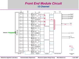
CZT FRONT END ELECTRONICS INTERFACE I/O signal CZT ASIC FRONT END ELECTRONICS TO PROCESSING ELECTRONICS +/-15V -500 V BIAS +/-2V
FEATURES OF ASIC XaIm3.2 • It is fully data driven charge signal acquisition chip. • 2. All Analog and Digital outputs are current driven for 1µs. • Each pixel is addressable. • 3.Provision of programming for needed parameters of the chip like threshold, shaping time constant and various other parameter. • ClkIn and RegIn are Clock and Input for the Shift-registor. • 4. The chip requires +2 and -2 volts for operation. • 5. Daisy chaining of chips.
Outline of Amplifier channel in aout ctout
Data acquisition in ASIC at each event • Hit pixel collected charge pulse is amplified & filtered in pre-amp & shaper. • Peak detector detects the peak of the pulse. • If peak value is larger than threshold, trigger signal will be generated. • Hit pixel trigger signal + Analogue peak value + Channel address. (Readout period = 1µs). • The chip resets itself after Readout period.
3 2 1 REG IN REG IN REG IN REG OUT REG OUT REG OUT CLK IN CLK IN CLK IN • DAISY CHAINING OF ASIC • Upto 512 chips can be daisy chained on a common shared bus. • Options for us:- • 128 individual lines for each ASIC. • 128 ASIC daisy chained. • 32 ASIC daisy chained, so 4 quadrant.(32 x 4)
ASIC Specifications • Power Rails : DVdd = +2V,DVss = -2V AVdd = +2V,AVss = -2V • Read out = Self triggered & data driven • Analog output = 0-200 µA • Read out time = 1 µS • Channels = 128 • Peaking time = Nominal : 0.5 µS Adjustable : 0.35 µS – 1 µS • Power Dissipation = 3.2 mW / channel • Can be easily daisy chained.
M1 M2 M3 Mn DATA CLOCK ADDR BUS DATA BUS TRIG & MULTI HIT ENERGY PULSE