The chip Signal processing for High Granularity Calorimeter
180 likes | 367 Vues
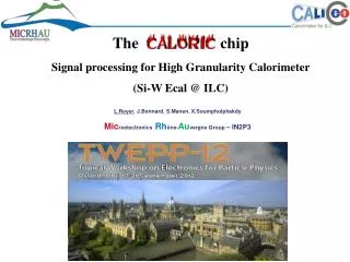
The chip Signal processing for High Granularity Calorimeter (Si-W Ecal @ ILC). L.Royer , J.Bonnard , S.Manen , X.Soumpholphakdy Mic roelectronics Rh ône- Au vergne Group – IN2P3. The I nternational L inear C ollider.

The chip Signal processing for High Granularity Calorimeter
E N D
Presentation Transcript
The chip Signal processing for High Granularity Calorimeter (Si-W Ecal @ ILC) L.Royer, J.Bonnard, S.Manen, X.Soumpholphakdy Microelectronics Rhône-Auvergne Group – IN2P3
The InternationalLinear Collider ILC “could be the next big adventure in particle physics” “It would complement the LHC at CERN and shed more light on the discoveries scientists are likely to make there in the coming years.” [http://www.linearcollider.org/] (Credit: Greg Stewart, SLAC) Time structure of the ILC: • Bunchtrainsof 2820 bunches spaced 337 ns • Each bunch train is about 1 ms long • No beam during about 199 ms • Activity of the Very Front End Electronics: • During the beam activity: • analog signal processing (1ms) • A the end of the beam activity: • A-to-D signal conversion (.5ms max) • data transfer (.5ms max) • Idle mode during 198ms • about 99% of the time with no activity for electronics on detectors ILC BEAM STRUCTURE A/D conv. DAQ IDLE MODE Analog electronics busy 1ms (.5%) .5ms (.25%) .5ms (.25%) 198ms (99%)
Challenges for the Si-W Ecal • Sandwich structure of thin wafers of silicon diodes & tungsten layers • Embedded Very Front End (VFE) electronics • Deeply integrated electronics • Minimal cooling available • High granularity : diode pad size of 5x5 mm2 • High segmentation : ≈ 30 layers • ≈ 100.106 channels • Large dynamic range of the input signal (≈ 15 bits) ILC Calorimeters « Tracker electronics with calorimetric performance »
Readout Electronics for the Si-W Ecal • Specifications of the readout electronics of Ecal: • Dynamic range of the signal delivered by a Si-diode : from MIP (4 fC) to 2500 MIPs (10 pC) • Level of noise limited to 1/10 MIP SNR ≈ 10 • Error of Linearity: • < 0.1 % up to 10 % of the dynamic range (1 pC) • < 1% from 10 % and 100 % of the dynamic range (10 pC) • Power budget limited to 25µW per channel • Power Pulsing must be implemented 4
First prototype readout channel • Axes of development @ MicRhAu: • Synchronous/clocked (with beam) analog signal processing: reseted-CSA, shaping with Gated Integrators including the analog memory, latched comparators • Fully differential architecture, except for the Charge Sensitive Amplifier (CSA) • One low-power ADC attached to each channel (12-bit cyclic ADC) • Use of a pure CMOS technology, no bipolar transistors (low cost AMS CMOS 0.35 techno.) Cyclic ADC CSA • Some results: • Global Linearity better than 0.1 % (10 bits) up to 9.5 pC (2375 MIP). • ENC = 1.8 fC (0.5 MIP) with a single gain stage • Power consumption with power pulsing estimated to 25µW • Results published in IEEE TNS (ISSN : 0018-9499) 5
The CALOrimetryReadout Integrated Circuit (1/4) 4 ADC Low noise CSA Low-gain shaper 12-bits cyclic ADC • Based on the previous validated prototype, a new chip designed • Technology AMS CMOS 0.35 µm • Architecture of CALORIC based on the previous channel tested, with some improvements: • Reduction of the power consumption of the CSA • Reduction of the noise of the amplifier of the Gated Integrator • Increase of the analog memory depth to 16 • Chip fully power pulsed 6
The CALOrimetryReadout Integrated Circuit (2/4) x16 Gain discri. 4 ADC Low noise CSA High-gain shaper Low-gain shaper 12-bits cyclic ADC x16 • Threshold • A High-Gain (about x 20) channel added to improve the SNR at low energy • A discriminator indicates the dynamic range of the signal select the signal to be converted 7
The CALOrimetryReadout Integrated Circuit (3/4) x16 Gain discri. Trigger discri. 4 ADC Low noise CSA High-gain shaper High-gain shaper Low-gain shaper Amplifier 12-bits cyclic ADC x16 x5 • Analog part • A Trigger channel added to auto-select events over the MIP • The trigger signal determinates if the active memory cell is reset or the signal kept into memory • Threshold 8
The CALOrimetryReadout Integrated Circuit (4/4) Gain discri. Trigger discri. x16 ADC 4 Low noise CSA Low-gain shaper High-gain shaper High-gain shaper Amplifier 12-bits cyclic ADC x16 • Digital Block • (State Machine) 12 • Output • data x5 • Analog part • A digital block controls the chip • Thresholds • Control of the channel 9
Global State Machine IDLE WAIT for 198 ms No power At the end of idle time, digital state machine wakes up and isready to manage new events. Wake Up Analog signal processing 1 ms max. Up to 16 events stored End of the bunch trains Bunch Crossing A/D conversion Time conversion < 1 ms x events stored Master clock of 20 MHz (period of 50 ns) All events converted DAQ (not implemented) A/D conv. DAQ IDLE MODE Analog electronics busy 1ms (.5%) .5ms (.25%) .5ms (.25%) 198ms (99%) 10
Timing of the analog processing Bunchperiod = 350 ns Signal delivered by the Si-diode Output signal of the CSA Output signal of the trigger channel Output signal of high-gain channel Output signal of the low-gain channel t = 0 ns: bunch crossing (event synchronous w/ beam) + 200 ns: activation of the trigger comparator + 250 ns: activation of the gain comparator + 300 ns: end of integration: reset or memorization 11 + 350 ns: ready to process next event
Layout of CALORIC_1ch GatedIntegrator and the 2x16 memory cells CSA, trigger channel and comparators The cyclic ADC The digital block Channel area in AMS 350nm : 1.2 mm² 12
Main Performance of Caloric_1ch • Most functionalities are validated: charge is collected, converted to voltage, amplified, filtered, memorized and digitally converted; the digital block manages well the sequencing of the signal processing • Trigger channel non-functional signal dominated by noise (digital signals) and too large offset • Bug on the routing of power pulsing signal • ENC (rms value) with CD=30 pF: 0.6 fC(3750 e-) • MIP-to-noise ratio 6 • Integral Non-Linearity: • < 0.2% up to 0.4 pC • < 1% from 1 pC to 6 pC • Gain dispersion for 16 memory cells : • 1.5% (rms value) the low-gain • 2.5% for the high-gain • Results published in IEEE TNS (ISSN : 0018-9499) ENC= 0.6 fC
Power consumption of Caloric_1ch • Evaluation using power pulsing with the ILC duty cycle: 43 µW/channel CSA Trigger channel High Gain channel Low Gain channel 14
Caloric_4ch (1/3) • 4-channel chip designed • Power pulsing bug corrected • New amplifier for the trigger channel less sensitive to process& mismatch fluctuations • Gated integrator: Time-variant system Noise simulations performs both with transient noise and periodic noise tools from Cadence • Results in accordance (difference < 10%) • MIP/noise=10 for trigger channel Spectral density of the noise for the trigger channel Output signal of the trigger channel on MIP event vs process/mismatch fluctuation Simulated noise: MIP/10 Threshold voltage
Caloric_4ch (2/3) Minimizing noise coupling from the digital part to the analog part MIP/10 = 0.4fC equivalent to a voltage step of 3.3V on a 0.12 fF capacitor !! • Shapers & ADC fully differential to reduce sensitivity to common-mode noise • Few “common sense rules” implemented for the layout to minimize noise coupling: • Analog and digital blocks isolated from one another with free-space and p+ guard rings • Analog and digital blocks with own independent power supply • Complementary signals for clock to minimize injection to analog signals • Several Pads per each power supply to reduce the inductance of bounding wiring • On-chip decoupling capacitors • Sensitive analog signal lines far away from perturbing lines • Digital pads with high toggle rate placed far from analog domain • Package have to be carefully chosen
Caloric_4ch (3/3) Submission to the next AMS run in November Channel 1 Channel 2 (2.7 x 2.7) mm2 Decouplingcapacitors Channel 3 Channel 4
Conclusion • We have designed a pure CMOS–differential-synchronous readout electronics dedicated to the Si-W Ecal of ILC. • All the functionalities have been tested and most are validated: amplification, filtering, memorizing, A-to-D conversion, global state machine for sequencing. • But two main functionalities are missing: the auto-triggering and the power pulsing. They will be tested with Caloric-4ch. • This work shows the difficulties to detect and process very small charge (<1fC) inside a mixed analog/digital chip. A technology with higher resistivity substrate (BFMOAT with 130nm IBM RF technology) should be better suited for mixed-signal design. • Power consumption must be divided by a factor 2 to reach requirements of ILC. It is not a trivial issue but improvements must be focused on the amplifiers. • This development provides us successful experiences in the design of low noise CSA, time-variant filtering, A-to-D converters, mixed chip, …. • This experience will be useful for the present and future projects @ MicRhAu. THANK YOU ! 18