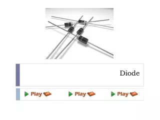
Step Recovery Diode
Step Recovery Diode. Group Members. Muhammad Ahsan Majeed 2011 –ee-594 Qaisar Khalil 2011-ee-595 Muhammad Usman 2011-ee-596 Muhammad Faizan 2011-ee-597 Azhar Naeem 2011-ee-598 Muhammad Nouman 2011-ee-599 Samina Bibi 2011-ee-600 . Definition & introduction


Step Recovery Diode
E N D
Presentation Transcript
Group Members • Muhammad AhsanMajeed 2011 –ee-594 • QaisarKhalil 2011-ee-595 • Muhammad Usman 2011-ee-596 • Muhammad Faizan 2011-ee-597 • AzharNaeem 2011-ee-598 • Muhammad Nouman 2011-ee-599 • SaminaBibi 2011-ee-600
Definition & introduction • Construction & fabrication • Types & symbol • Operation • Graphical representation • Specification • Applications
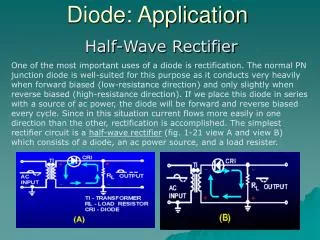
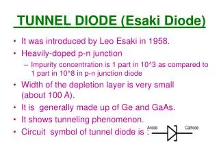
Definition & introduction A heavily doped diode with an ultrafast switching time. The step recovery diode is an ultrafast diode like the pin diode. • Step recovery diode or srd is also used as high order multiplier and will multiply as high as 20x when used as a comb generator.
Step recovery diodes ( SRD's ) are used primarily in generating extremely fast rise time pulses • for use in frequency comb generation, harmonic frequency multipliers and samplers. In most applications, the SRD is used as a charge controlled switch. • When forward biased, charge is injected into the diode making it a low impedance. • When the stored charge is removed, the diode continues to have a low impedance until all the charge is removed at which point, the diode rapidly switches from the low to a high impedance. • The SRD is designed to have the fastest transition
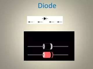
CONSTRUCTION • The step recovery diode is fabricated with the doping level gradually decreasing as the junction is approached or as a direct PIN structure. This reduces the switching time because there are fewer charge carriers in the region of the junction and hence less charge is stored in this region.
STEP RECOVERY DIODE In the step recovery diode the p and n type material are much dopped heavily at the end of the component then there at the junction.
The step-recovery diode is also used for fast switching applications. This is achieved by reduced doping at the junction. ET212 Electronics – Special Purpose Diodes Floyd 29
operation • The step recovery diode is used as what is termed a character controlled switch. When the step recovery diode is forward biased and charge enters it, the diode appears as a normal diode and it behaves in much the same way. • When diodes switch from forward conduction to reverse cut-off, a reverse current flows briefly as stored charge is removed. When all the charge is removed it suddenly turns off or snaps off. • It is the abruptness with which the reverse current ceases that enables the step recovery diode to be used for the generation of microwave pulses and also for waveform shaping
Specifications: (@ +25°C, 0.5 Watt Input) INPUT 2 MAX MINIMUM OUTPUT POWER PER PICKET (dBm) 1 MODEL FREQ. INPUT 3 (MHz) VSWR UP to 4 GHz 4-8 GHz 8-12.4 GHz 12.4-18 GHz 18-26 GHz GC100** 100 2:1 -10 -20 -30 -40 ---- GC200** 200 2:1 -5 -15 -25 -35 ---- GC250** 250 2:1 0 -10 -20 -30 ---- GC500** 500 2:1 +5 -5 -15 -20 ---- GC1000** 1000 2:1 +5 0 -10 -15 ---- GC0526** 500 2:1 +5 -5 -15 -20 -40 GC1026** 1000 2:1 +5 0 -10 -15 -35 GC1526** 1500 2:1 +5 0 -5 -10 -25 GC2026** 2000 2:1 +5 +5 0 -10 -20
Specification (SRD) • Note 1: • Suffix (**) specify options for internal DC return and package style. First Position: N indicates no DC return and R indicates internal DC return included. Note that DC Return is required for proper operation. Second Position: C, L, or Y indicates Package style (see outline drawings page) • Note 2: • Other input frequencies from 10 MHz to 10 GHz are available. Contact factory for information. • Note 3: • For second harmonics up to 4 GHz the fundamental feedthrough is typically +15dBm.
Note 4: • All units can respond to a 3% bandwidth of input frequency without noticeable degradation. • Note 5: • All models can be modified for use as an impulse generator. Consult factory for information on output amplitude, polarity, and pulse width. • Note 6: • Add “X” to final suffix for an enhanced assembly version for more severe vibration environment.
APPLICATIONS • Impulse Generator • Frequency Multipliers • Frequency Synthesizers • Built-In-Self-Test Sources
General Applications Information • This section provides general guidance in connecting a variety of loads to the outputs of ultra-fast rise time AVTECH pulse generators (100 ps to 1 ns). Fifty Ohm loads, low impedance loads such as laser diodes, and high impedance loads such as CRT and photomultiplier grids are considered in particular.
The use of Avtech bias insertion units, matching transformers, inverting transformers, low-impedance AV-LZ lines and power splitters is also discussed. The application of AVTECH pulse generators to pulsed laser diode driving and to switching time testing of semiconductor diodes and transistors is included as well
. But to begin with, we first define the pulse parameters rise time and pulse width and we then consider the topics of oscilloscope bandwidth and the probing of ultra high speed voltage and current waveforms.