Download

1 / 7
70 likes | 285 Vues
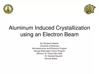
starting substrates were undoped 5 m m thick GaN films grown by hydride vapor phase epitaxy (HVPE) on c -plane sapphire. 60 nm thick SiO x film was then deposited on the GaN film using an electron beam evaporator. 1 m m thick Al film was deposited.

E N D
starting substrates were undoped 5 mm thick GaN films grown by hydride vapor phase epitaxy (HVPE) on c-plane sapphire. 60 nm thick SiOx film was then deposited on the GaN film using an electron beam evaporator 1 mm thick Al film was deposited anodization was then carried out to create porous anodic alumina (PAA) PAA template serves as a mask to transfer the pore pattern into the SiOx layer GaN nucleates on PAA under conventional growth conditions BUT GaN does not readily nucleate on silica --> thereby allowing for selective growth only in regions of exposed substrate
PAA was pore widened from ~10 nm to 60 nm (see Fig 1a) sample was subjected to reactive ion etching (SF6 and O2, were gases used) PAA was then removed with by immersing the sample in a 5 vol % H3PO4 solution at 50°C for 60 min (see Fig 1b)
the GaN nanorods were grown from the GaN substrate, through the pores in the SiOxtemplate the growth was done using organometallic vapor phase epitaxy (OMVPE) the SiOx film was removed by immersing the sample in a buffered oxide etch for 20 s
prismatic faceting along with a pyramidal cap formed during the self-terminated growth as the nanorod grew beyond the silica template with increased growth time, the nanorod tip came out of the silica template and started growing laterally (but still maintained the pointed tip morphology)
SUMMARY demonstrated a new nonlithographic and catalyst-free technique for controllably growing GaN nanorods in place possible nanophotonics applications due to the high-aspect-ratio form factor and the quantum confinement
SUMMARY “The Heterogeneous Integration Research Group was recently funded by the NSF to exploit the elastic strain relief in nanorod heterostructures in extending the spectral range of (In,Ga)N LEDs from uv-blue-green toward amber and red. Today’s (In,Ga)N LEDs are familiar as the green traffic lights with the intense color and pixilated appearance. Bright blue (In,Ga)N LEDs are also manufactured in high volume, and are widely employed in cell phones. These blue LEDs combined with a yellow phosphor are also used in the first generation of white LEDs. The Purdue effort is focused on understanding the relationship between strain and InN incorporation in “quantum disks” grown within (In,Ga)N nanorods, with the ultimate aim of demonstrating emission of light across the full visible spectrum from a single nanostructured heterostructure, without phosphor downconversion. Graduate students Parijat Deb (MSE), Sangho Kim (ECE) and HoGyoung Kim (Physics) are working together to investigate the epitaxial growth of (In,Ga)N nanorod arrays using OMVPE and a custom-built halide vapor phase epitaxy (HVPE) reactor.” https://engineering.purdue.edu/MSE/Features/TheNextSolidStateRevolutionEnergy Sands Group Website: https://engineering.purdue.edu/MSE/Fac_Staff/Faculty/TURNER_LAB/index_html/