Download
1 / 1
10 likes | 220 Vues
tip. lens. V. V+V AC. laser. 1nm. Raman. I. I+I AC. surface. 0.5nm. molecule. adsorbate. tip. metal. insulator. metal. Magnetism of Few-Atom Clusters on Ultrathin Insulating Films David Gohlke, Taeyoung Choi, Jay Gupta – The Ohio State University, Department of Physics. Cu 2 N.

E N D
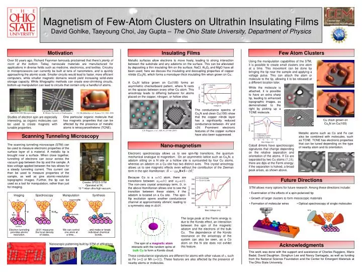
tip lens V V+VAC laser 1nm Raman I I+IAC surface 0.5nm molecule adsorbate tip metal insulator metal Magnetism of Few-Atom Clusters on Ultrathin Insulating FilmsDavid Gohlke, Taeyoung Choi, Jay Gupta – The Ohio State University, Department of Physics Cu2N 1nm Few Atom Clusters Motivation Insulating Films Metallic surfaces allow electrons to move freely, leading to strong interaction between the substrate and any adatoms on the surface. This can be alleviated by depositing a thin insulating film on the surface. NaCl, Al2O3 and MgO have all been used; here we discuss the insulating and decoupling properties of copper nitride (Cu2N), which forms a monolayer-thick insulating film when grown on Cu. Over 50 years ago, Richard Feynman famously proclaimed that there’s plenty of room at the bottom. Today, nanoscale materials are manufactured for applications in diverse fields such as medicine, electronics, and textiles. Circuitry in microprocessors can currently be built at tens of nanometers, and is quickly approaching the atomic scale. Smaller circuits would lead to faster, more efficient computers, while smaller magnetic domains would yield increasing solid-state storage capacity. While lithographic methods can create ever-shrinking circuits, bottom-up manipulation can lead to circuits that contain only a handful of atoms. Using the manipulation capabilities of the STM, it is possible to create small clusters one atom at a time. This movement can be done by bringing the tip near the sample and applying a voltage pulse. This can attach the atom or molecule to the tip, allowing it to be released at a different location later. A Cu2N lattice grown on Cu(100) forms an asymmetric checkerboard pattern, where N rests on the spaces between every other Cu atom. This anisotropy leads to differing behavior for atoms placed on the copper, nitrogen, or hollow sites While the molecule is attached, it is possible to have an extra sharp tip, leading to enhanced topographic images, as demonstrated to the right by picking up a TCNE molecule. Co TCNE The conductance spectra of Cu2N and clean Cu(100) show that the copper nitride layer has a significantly reduced conductance between -4V and +2V. Prominent electronic features of the copper surface have also been suppressed. Intel 80486 DX2 Microprocessor H. Mizuta, University of Southampton C.F. Hirjibehedin et al., Science 312, 1021, 2006 One particular organic molecule that has magnetic properties that can be affected by the presence of metallic atoms is tetracyanoethelene (TCNE). Studies of electron spin are especially interesting, as organic molecules can be used to create magnets with tunable properties. Co Cu chain grown on Cu2N on Cu(100) C.D. Ruggiero, et al., APL 91, 253106 (2007) Metallic atoms such as Co and Fe can also be combined with molecules, such as TCNE. TCNE has electronic properties that can be tuned depending on the type of nearby atom and its orientation. Scanning Tunneling Microscopy Nano-magnetism The scanning tunneling microscope (STM) can be used to measure electronic properties of the surface layer of a material. A metallic tip is brought near a surface. When close together, tunneling of electrons can occur across the vacuum gap between the tip and the sample. A bias voltage applied between the two allows for a steady tunneling current. This current can then be used to measure properties of the sample, as well as give atomic-resolution topographic images. Further, the tip can be used as a tool for manipulation, rather than just for imaging. Cobalt dimers have spectroscopic signatures that change depending on the relative separation and orientation of the atoms. If Co are separated by two Cu atoms (7.2Å), there are dips at the Fermi energy; if the separation is halved, a broad peak arises, as shown above. Electronic spectroscopy allows us to see spin-flip transitions, the quantum mechanical analogue to magnetism. On an asymmetric lattice such as Cu2N, a adatom sitting on a N site or a hollow site is surrounded by four Cu atoms, whereas an adatom on a Cu site has two distinct axes. This crystal anisotropy allows us to see magnetic effects even without the contribution of the Zeeman term in the spin Hamiltonian: 1nm Fe(TCNE) Fe Because Co is a s=3/2 atom, there are transitions between ms=±3/2 and ms=±1/2. The non-zero crystal anisotropy term, D, in the above Hamiltonian allows one to see the transition between these states, if the adatom is located on a Cu site. This spin-flip excitation opens another conductance channel at approximately ±6meV, leading to a symmetric step in dI/dV. Future Directions Createc SPECS STMOperated at 5K, 10-10 mbar ultra-high vacuum. • STM allows many options for future research. Among these directions include: • Examination of the effects of a spin-polarized tip • Growth of larger clusters to form mesoscopic materials • Formation of molecular wires Imaging Spectroscopy Manipulation Synthesis • Optical spectroscopy of single molecules The large peak at the Fermi energy is due to the Kondo effect, an interaction between the spin of the magnetic adatom and the electrons of the bulk Cu. The dependence of the Kondo resonance on the anisotropy of the system can also be seen, as a Co atom on the N site does not exhibit this feature. Electron tunneling provides atomic resolution. dI/dV measures the local density of states. We can control one atom at a time… …and make or break individual chemical bonds. Acknowledgments The spin of a magnetic atom interacts with the random spins of bulk Cu to form a Kondo cloud. Nanoscopic patterning built by STM of affiliations This work was done with the support and assistance of Charles Ruggiero, Mario Badal, David Daughton, Donghun Lee and Nancy Santagata, as well as funding from the National Science Foundation and the Center for Emergent Materials at The Ohio State University. These conductance signatures are different for atoms with other values of s, such as Fe (s=2) or Mn (s=5/2). These features are also affected by the presence of nearby atoms or molecules.