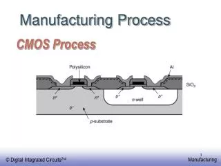
UNIT 5: CMOS subsystem design
UNIT 5: CMOS subsystem design. ( Pucknell p:-134-178) ( Neil west - p:-317-357). Switch logic Gate logics Combinational logic Clocked sequential circuits Clocking Strategies,PLL. Introduction. Large systems are composed of sub-systems, known as Leaf-Cells


UNIT 5: CMOS subsystem design
E N D
Presentation Transcript
UNIT 5:CMOS subsystem design (Pucknellp:-134-178) (Neil west -p:-317-357)
Switch logic • Gate logics • Combinational logic • Clocked sequential circuits • Clocking Strategies,PLL
Introduction • Large systems are composed of sub-systems, known as Leaf-Cells • The most basic leaf cell is the common logic gate (inverter, nand, ..etc) • Structured Design • High regularity • Leaf cells replicated many times and interconnected to form the system • Logical and systematic approach to VLSI design is essential
Architectural issues • In all design process, a logical and systematic approach is essential • Define the requirements • Partition the overall architecture into appropriate subsystems • Consider communication paths carefully • Floor plan :how the system is to map onto the silicon • Aim for regular structures • Draw stick or symbolic diagrams • Convert each cell to a layout • Carry out a design rule check on each cell • Simulate the performance of each subsystem
Switch Logic • Switch logic is based on the ‘pass transistor ‘ or on transmission gates. • Pass transistor • Gate(restoring) logic
Pass transistor and transmission-gate • switches and switch logic may be formed from simple n- p-pass transistors or from transmission-gate • Signal degradation occurs in Pass transistor logic • No Signal degradation occurs in transmission gate ,but more area is occupied S’ Vout Vin S S
Gate(restoring) logic • Gate logic is based on the general arrangement circuits • Ex : Inverter, Nand Nor, And, Or….
Vdd = 5V Vin Vout Vin Inverter • Some of the commonly used inverter circuit diagrams Vdd = 5V Vout
nMOS inverter 2λ 2λ 2λ 16λ 8λ 4λ
Nand gate two significant factors • nMOS Nand gate area requirement: As inputs are added, so must there be a corresponding adjustment of the length of the pull-up transistor channel to maintain the required overall ratio • nMOS Nand gate delay: For n inputs, then the length and resistance of the pull-up transistor must be increased by factor of n to keep correct ratio. Delay associated with the nMOS Nand gate ГNand=nГ
Since both transistor of the nMOS Nor gate provide a path to ground from the pull-up transistor, the ratios must be such that any one conducting pull-down transistor will give the appropriate inverter-like transfer characteristic.
Pseudo-nMOS logic • The circuit is replaced by depletion mode pull-up transistor of the standard nMOS circuits with a p-transistor with gate connected to Vss. • Ex: 3 input NAND gate..
Dynamic CMOS logic • Charge sharing problem unless the inputs are constrained not to change during the on period of the clock • Single phase dynamic logic structures cannot be cascaded
Clocked CMOS logic • Logic is implemented in both n- and p-transistors in the form of a p-block and n-block structure • The logic is evaluated only during on period of the clock
n-p CMOS logic • The actual logic blocks are alternately ‘n’ and ‘p’ in a cascaded structure • Logic operation depends on clock φand clock bar φ’ alternatively
Examples of structured design (Combinational logic) • A parity generator • Bus arbitration logic for n-line bus • Multiplexers (Data selectors) • A general logic function block • A four-line gray code to binary code converter • The programmable logic array (PLA)
Parity generator P • Ai=1 parity is changed, Pi=P’i-1 • Ai=0 parity is unchanged, Pi=Pi-1 P’ A0 A1 A2 An-1 An P=1 even number of 1’s at input P=0 odd number of 1’s at input
Stick diagram Pi P’i P i-1 P’ i-1 A’i Ai
Bus arbitration logic for n-line bus • If the highest priority line An is Hi (logic 1), then output line Apn will be Hi and all other output line Lo (logic o), irrespective of the state of the other input lines A1----An-1. • Similarly , Apn-1 will be Hi and all other output line Lo (logic o), irrespective -1 will be Hi only when An-1 is Hi and An is Lo; again the state of all input lines of lower priority (A1----An-2)will have no effect and all other output lines will be Lo.
n-line bus Stick diagram Apn An Apn-1 An-1 0 An-2 Apn-2 0 0 A’n-1 An A’n An-1
Multiplexers (Data selectors) I0 I1 I2 I3 MUX Z S1 S’1 S0 S’0
MUX Stick diagram Z I0 I1 I2 I3 S1 S’1 S0 S’0
A general logic function block A’ A B’ B Select inputs Z Nor, Nand Data inputs C3 C2 C1 C0 0 0 0 1 0 1 1 1
A four-line gray code to binary code converter • A0=G0A1 • A1=G1A2 • A2=G2A3 • A3=G3 } Exclusive-or operations
System Considerations Lose sight of overall system requirements and restrictions Use of buses to interconnect subsystems and circuits must always be most carefully considered. Bipolar drivers for Bus Lines Basic arrangements for Bus Lines Power dissipation for CMOS and BiCMOS circuits Current limitations Further aspects of Vdd and Vss rail distribution
Bipolar drivers for Bus Lines • Bus structures carrying data and control signals are generally long and connected to and trough a significant number of circuits and subsystems • Propagation of signals may be a slow process • The capacitive load driving properties of bipolar transistors in a BiCMOSprocess make bipolar drivers an attractive proposition for bus lines
Basic arrangements for Bus Lines • There are three classes of bus- passive ,active and precharged • A passive bus rail is a floating rail to which signals may be connected from drivers through series switches
In active bus a common pull-up Rp.uand n-type pull-down transistors or series n-type transistor logic
The Precharged bus concept • The precharged bus approach limits the effects of bus capacitance in that a single pull-up transisterwhch is turned on only during 2
Power dissipation for CMOS and BiCMOS Circuits • The overall dissipation is composed of two terms: • P1 the dissipation due to the leakage current I1 through an ‘off’ transistor. Consequently, for n transistors, we have P1=n.I1.Vdd Where I1=0.1 nA, typically at room temperature. • Ps is the dissipation due to energy supplied to charge and discharge the capacitances associated with each switching circuit Ps=CL.Vdd2.f • Total power dissipation Pt=P1+Ps • Power dissipation for bipolar devices can be simply modeled by P=Vcc* Ic • Ic is the current through the device
Current limitations for Vdd and GND rails • Metal migration for high current densities in metal conductors • Aluminum conductor threshold value Jth=1 to 2 mA
Further aspects of Vdd and Vss rail distribution • Limitations of distributive rails are: • Metal migration imposed current density restrictions • The IR drop due to rail series resistance • The series inductance of the rails
IR drop and series inductance • For a parent bus supplying current to other uniformly distributed short bus branches along the length L of the parent bus, then the current at any distance x from the source is given by Ix=IL(1-x/L)
series inductance • The transmission line nature of any wiring introduces the possibility of voltage transients due to its self-inductance L0. the transient changes in voltage due to the presence of self-inductance can be modeled by ∆V=L0 di/dt di/dtIs the rate of change of line current