Download
1 / 32
320 likes | 455 Vues
Scanned Probe Imaging of Switching Centers in Molecular Devices. HP Labs Quantum Science Research. Chun Ning (Jeanie) Lau Dr. Duncan Stewart Dr. R. Stanley Williams Prof. Marc Bockrath (Caltech). Molecular Electronics. Challenges Fabrication Architecture New devices.

E N D
Scanned Probe Imaging of Switching Centers in Molecular Devices HP Labs Quantum Science Research Chun Ning (Jeanie) Lau Dr. Duncan Stewart Dr. R. Stanley Williams Prof. Marc Bockrath (Caltech)
Molecular Electronics • Challenges • Fabrication • Architecture • New devices • Ultimate limit of miniaturization • Self-assembly low fabrication cost
Fault-tolerant Architecture Nano-imprint Lithography • fast fabrication of nm scale features over cm area HPL TeraMAC 1 THz multi-architecture computer • Largest defect-tolerant computer • 220,000 (3%) defective components • 106 gates operating at 106 cycle/sec • addresses problem of <100% yield Heath et al, Science (1997). 6 Gbits/cm2 Y. Chen, G.Y. Jung et al. (2003).
Molecular Switches • Potential applications as memory or logic devices • Previously studied systems: Nanopore, STM, cross-bar • Molecules studied: rotaxane, catanane, OPE, etc Unsolved Question • What are the switching mechanism(s)? • Proposed: • conformational change of molecules • eletrical charge transfer, electron localization • molecule-metal contacts
Switching of Metal/Alkane/Metal Junctions • Stearic acid: • electrical insulator HOMO-LUMO gap ~ 8eV • no redox centers, mobile subgroups, or charge reception sites C H O 1 8 3 6 2 Langmuir-Blodgett films of molecular monolayer sandwiched between mm-sized metallic electrodes 2.6 nm H O C O Ti Pt H C 3 Our Experiment
Switching of Metal/Alkane/Metal Junctions 1000 500 A) (m 0 Current -500 -1000 -0.5 0.0 0.5 1.0 Voltage (V) A V 1 2 Ti 3 Pt 4 • Asymmetric electrodes (Ti & Pt) • Reversible switching dependent on bias direction Stewart et al, Nano Lett., in press.
Novel Scanned-Probe Technique AFM Ti Pt Si Substrate • Apply ~mN force with AFM tip while measuring device conductance • Simultaneously explores electrical and local mechanical properties • AFM tip not electrically connected to the device
AFM Imaging of Mechanically-induced Conductance Response • Plot conductance through junction as a function of tip position • AFM tip applies ~mN force pressure ~ 103 – 104 atm
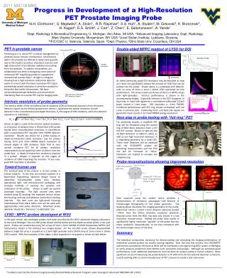
Conductance Map (“off” state) on off A V Topography off Conductance (Off) 15 mm Molecular junction in the “off” state exhibited no observable electrical response to local mechanical perturbation by the AFM tip.
Conductance Map (“On” state) on off Conductance (Off) Topography Conductance (On) 15 mm • A nanoscale conductance peak (“switching center”) emerges when the junction turn “on”.
400 on 200 on Off Off Off (mA) 0 I -200 1.0 0.5 -400 50 nm 0.0 (mA) -0.4 -0.2 0.0 0.2 0.4 I -0.5 Vbias -1.0 -1.5 -0.4 -0.2 0.0 0.2 0.4 Vbias “Switching Centers” Switching “on” of a device is always accompanied by the emergence of a new nanoscale pressure-induced conductance peak.
Switching “off” 1.6 300 1.5 200 1.4 (mA) 1.3 I 100 (mA) 1.2 I 0 0.050 0 1 2 3 4 Vbias 0.045 0 2 4 6 8 10 m Tip Position ( m) 1 2 3 1 The switching center faded and completely vanished with successive switchings to lower conductance states. 2 3
Our Experimental Finding Lau et al, in preparation. • Under mechanical pressure, a single nanoscale conductance peak (switching center) appears when the junction is switched “on”, and disappeared when “off”. • Formation and dissolution of nanoscale structural inhomogenities on the junction give rise to switching. What are these inhomogenities?
A Simple Model • Transport across molecular monolayer via tunneling • When switched “on”, electrodes move closer together within a nanoscale region dominate transport • Conductance only increase when the AFM tip is compressing the nano-asperity. Nano-asperity (top or bottom electrodes)
Applying Pressure with AFM tip F z=0 d Elasticity theory (Landau&Lifshitz) point force applied to semi-infinite plane strain at (x,y,d) E = Young’s modulus ~ 80 GPa for metals and alkane molecules d = thickness of top electrode ~ 30 nm • Monolayer compressed by dz (~ 0.2 Å for F ~ 1 mN) • Spatial resolution ~ 40 nm : Limited by tip radius and thickness of top electrode.
A Simple Model Model Data G = Goff + (Gon-Goff )exp (- b dz(x, y)) • Nano-asperity dominate transport nano-asperity located at (0,0) “off” state conductance 1.2 mS 1.4 No free parameters : Goff~ 0.1mS, Gon~1.3mS, b~1Å-1, dz (0,0) ~ 0.2 Å • Good agreement between model and data • switching “on” ↔ growth of asperity
Nanoscale Filaments 400 on 200 Off Off (mA) 0 I -200 -400 860mS 850 -0.4 -0.2 0.0 0.2 0.4 Vbias On/off ratio ~ 105 • G>>conductance quantum GQ Continuous filamentary pathway • switching ↔ formation and dissolution of nano-filaments • Nature and growth mechanism of filaments? • (thermal migration, electrochemical reaction, electro-migration…)
Effect of Force on Conductance tunnel barrier 600 nm Force Current 0.1 mN Conductance within a “switching center” increases with increasing applied force. 0.6 mN 1.5 mN 3 mN Vbias = 0.1 V
Conclusion • Novel experimental technique that probes nanocale conductance pathways through molecular junctions • New switching mechanism with high on/off ratio due to formation and break-down of conductive nano-filaments Under Investigation • filament growth mechanism • pressure dependence • other systems (other molecules, different electrodes) • role of electrodes in metal/molecule/metal structures better engineering of molecule-based devices.
mastery of nanoscale systems • molecular devices • superconducting nanowires & nanorings • ferromagnetic nanowires • single molecules • carbon nanotubes • nanosensors • …… We’re only at the base camp….
Silicon ElectronicsWires & SwitchesArchitectureLithography & DepositionComplex physical structurePerfect fabricationMemory & Logic NanoelectronicsWires & SwitchesChemical synthesis & assemblySimple physical structureImperfect fabricationArchitecture?Memory & Logic
Nanoscale filaments Nanoscale filaments grows or shrinks switching • Electromigration? • Elecrochemical migration? • Thermal migration? • Single dominant pathway Runaway process?
400 on 200 on Off Off Off (mA) 0 I -200 1.0 0.5 -400 0.0 (mA) -0.4 -0.2 0.0 0.2 0.4 I -0.5 Vbias -1.0 -1.5 -0.4 -0.2 0.0 0.2 0.4 Vbias “Switching Centers” Device A Switching “on” of a device is always accompanied by the emergence of a new nanoscale pressure-induced conductance peak.
1.3 S) (m G 1.2 0 250 Tip Position (nm) Nanoscale Filaments? Device A Device B • Unperturbed conductance ~ 800 mS ~ 10 GQ • Small increase in conductance under pressure ~1% • Unperturbed conductance << GQ • Relatively large increase in conductance under pressure ~16%
Nano-imprint Lithography • nm scale features over cm area 6Gbits/cm2 Y. Chen, G.Y. Jung et al.
Fault-tolerant Architecture HPL TeraMAC 1 THz multi-architecture computer • Largest defect-tolerant computer • 220,000 (3%) defective components • 106 gates operating at 106 cycle/sec • Built from programmable gate arrays • Computes with look-up tables Philip Kuekes Collier et al, Science 1998.
Nano-imprint Lithography • fast fabrication of nnm scale features over cm area 6Gbits/cm2 Y. Chen, G.Y. Jung et al.
Tip position (mm) 19.0 R (kW) 18.0 0 2 Nano-conducting Channels Topography Top Electrode A local dominant nanoscale conducting channel Bottom Electrode Conductance image
Switching On of Molecular Junctions A conductance hot-spot appeared under mechanical modulation when the junction was switched on. • Diameter ~ 50 nm ~ AFM tip radius • 10% increase in conductance under ~2 mN
On 85.0 86.0 current (mA) Another Device Topography Conductance Off 1.025 1.112 1.200 Current (nA) On Off A new hot spotalways appeared after switching “on” the junction
Transport Through Molecular devices V Pt C18H36OH Pt T(K) Pt Ti 100 nm 2 mm diode r~5 x 10⁵ Stewart et al, in preparation. Chang et al, APL (2003) Single Molecule Measurements Nanoscale junctions
Molecular Electronics • Ultimate limit of miniaturization • Self-assembly low fabrication cost • “Designer molecules”