Analysis of 10V Vin and Vout Variations: Current and Error Estimates in Circuit Design
This document presents a comprehensive analysis of a 10V power supply circuit featuring different configurations across multiple parts. It includes detailed tables of current measurements (VBE and VGS) against Vin and Vout, alongside sketches representing the circuit layouts. Each segment concludes with error estimates to assess the accuracy of the measurements. The discussion also covers the performance of amplifiers, highlighting measured gains in common collector (CC) and common drain (CD) configurations, while providing insights into load effects with varying resistances.

Analysis of 10V Vin and Vout Variations: Current and Error Estimates in Circuit Design
E N D
Presentation Transcript
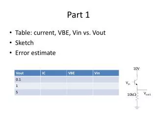
10V Vin Vout1 10kW Part 1 • Table: current, VBE, Vin vs. Vout • Sketch • Error estimate
10V Vin Vout2 10kW Part 2 • Table: current, VGS, Vin vs. Vout • Sketch • Error estimate • Measured gains CC and CD • discussion
10V Vin Vout3 1mA Part 3 10V RB Iout3 Iout4 M2 M4 M3
10V Vin Vout4 1mA Part 4 10V RB Iout3 Iout4 M2 M4 M3
Part 5 10V Vin 1uF Vload Vout4 1mA RL
Part 6 10V Vin VB RS Vout4 1mA
10V 10V 10V 10V Vin Vin Vin Vin Vout1 Vout2 Vout3 Vout4 10kW 10kW 1mA 1mA Q1 M1 M1 Q2 Q1 10V 10V 10V RB Vin VB Iout3 Iout4 Vin RS 1uF 1uF Vload Vout4 M2 M4 Vout4 M3 1mA 1mA RL