Part I: Amplifier Fundamentals
340 likes | 604 Vues
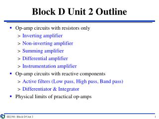
Part I: Amplifier Fundamentals. Agenda. Ideal Amplifiers Configurations and Operation of Amplifiers Common Amplifier Source Errors Understanding Amplifier Specification. Why So MANY AMPS???. Lots of Specifications Some are Important for Different Applications

Part I: Amplifier Fundamentals
E N D
Presentation Transcript
Agenda • Ideal Amplifiers • Configurations and Operation of Amplifiers • Common Amplifier Source Errors • Understanding Amplifier Specification
Why So MANY AMPS??? • Lots of Specifications • Some are Important for Different Applications • Each Amplifier is Designed to Improve or Optimize One or a Combination of Specifications • No Ideal Op Amp; YET? • Specialty Amps for a Variety of Applications and Functions • Current Amplifier Trends • Power Consumption - Driven by portable applications • Rail-to-Rail – Higher Dynamic range on lower supply voltage • Smaller Packaging – Circuit density in portable applications • Price – Higher Performance at lower Price
+ G X Y - What is an “Ideal” Op Amp? VIN • Amplifies a small signal (X) to a larger signal (Y) by Gain of G • Ideal Op Amp Characteristics • Voltage at + Input = Voltage at - Input • Infinite Input Impendence • Zero Output Impendence • Infinite Open Loop Gain • In closed loop Negative Input=Positive Input • Infinite Bandwidth VOUT
+ - Standard Configurations VIN Non-Inverting R2 VOUT R1 Inverting R2 VIN R1 + - VOUT
Operation of an “Ideal” Inverting Amplifier Virtual Ground Because +VIN = -VIN I2 R2 I1 Vin Vout + - R1
Operation of an “Ideal” Non-Inverting Amplifier Vin Vout + - R2 V1 I1 R1
Gain-bandwidth product • GBW product = Gain x BandWidth AOL 100000 GBP=1,000,000 10000 GBP=1,000,000 X 1000 ACL X 100 10 1
Nothing is ideal, friends.. • Real Characteristics • Finite open loop gain • Offset voltage • Input bias & offset currents • Finite bandwidth • And, these amplifiers are not free… IDEAL -+ REAL
-+ Input Error Sources • VOS – The difference in voltage between the inputs [~mV] Ideal Input Impedance (ZIN) Output Impedance (ZOUT) - A + Input Offset Current (Ios) Input Bias Current (Ib) Offset Voltage (Vos) • IB – The Current into the Inputs [~pA to mA] • IOS – The difference between the + IB and – IB [~IB /10] • ZIN – Input Impedance [MW to GW] • ZOUT – Output Impedance [<1W]
Bias Current Drift and Offset Voltage Drift • Offset Voltage is affected by the temperature • Drift is Usually in Units of mV/ ºC • Often a minimum and maximum VOS is Specified over the Temperature Range of the amp • Bias Current is also affected by temperature • Drift is Usually in Units of nA/ ºC • Often a minimum and maximum I BIAS is Specified over the Temperature Range of the amp • FET amplifiers have the lowest input Bias current
+ Very Low Bias CurrentFast FETs ™Amplifier Family Applications R2 • Photodiode Isc is linear over 6-9 decades and is usually in the range of pA-mA • Sensitivity is determined by amount of Isc multiplied by R2 • Minimizing Ib will ensure the highest possible sensitivity of the system • Additionally, maximizing the bandwidth minimizes the effects of Ib • Low DC Errors • Low Ibias, Vos and Drift • Low Noise • High-Speed Isc Ib AD8065 Precision Photo Diode Pre-Amp
Noise Gain • Noise Gain - gain of error signals (VER) between the inputs • Non-Inverting noise gain = Voltage Gain [R2/R1] • Inverting Noise gain = absolute value of the Voltage Gain +1 I R2 I Vout + - VER R1
All Input Error Sources End up at the Output • Input Referred Errors are multiplied by the Noise Gain • Initial VOS and VOS Drift Shift VOUT from the expected DC level • VOS drift multiplied by the change in temperature in ºC • Example: 2mV initial offset + 10mV/C with 100C shift and a gain of 5 creates 15mV offset at the output. • IB and IB drift with resistance (R1IIR2) at the summing node effectively create an additional VOS • Example: 10mA and R1 = R2 = 2k creates 10mV offset IB R2 IB=10mA Vout + - R1
Voltage or Current Noise Density CORNER FREQUENCY FREQUENCY Input Voltage and Current Noise • 2 Sources of Voltage and Current Noise • Low frequency Noise • Magnitude Increases as frequency decreases (1/f) • Wideband noise is flat over frequency • Usually Specified in Noise Density [nV/Hz and pA/Hz] • Multiply by the square root of the frequency range to determine the RMS noise • The intersection is referred to as the corner frequency
4V + 4mV - -4V 4V -4mV -4V Common Mode Rejection Ratio (CMRR) & Power Supply Rejection Ratio (PSRR) • CMRR is a ratio (output to input) of amplifier’s ability to reject an equal signal on both of the inputs • Similarly, PSRR is a ratio (output to power supply variation) of amplifier’s ability to reject power supply noise
Rail to Rail Amplifiers • Rail-to-rail amplifiers maximize signal swing, either on the input, the output or both. • True Rail-Rail op amps can swing to within a few mV of their power supply rails. • Non rail-to-rail op amps usually require between 1-3 volts of headroom to the supply rail • Analog Devices Rail to Rail Amplifiers • Rail to Rail Output • Fast FETsTM • AD8091/2 Very Low Cost, High-Performance • Rail To Rail Input • AD8031/2 Low Power High-Speed
Rail to Rail vs. Non Rail to Rail Amplifiers VIN +VS Out -VS In VOUT In +VS R-R Out -VS
Output Swing • Operating Region Decreases with Increased Frequency • Output Power [dBm] = 10log[V2rms/(RL)] x1mW Vout Saturation Increasing Frequency Vout Operating Region Iout Short Circuit Iout
Low-Power, Application Considerations • Minimize supply voltage circuitry or battery requirements • Reduce cooling requirements • Lower Heat Dissipation Saves Cost and Space • Smaller heat sinks • Essential in higher density PCB • Increases system stability and reliability • Example: • System with 5 AD8058 • (+/-5V)*(6.5mA/amp max)* (10 amps) = 650mW • Using AD8039 • (+/-5V)*(1.7mA/amp max)* (10 amps) = 170mW • ½ W Power savings
50 Open Loop Gain vs Freq.. 40 Gain 180 30 225 Degrees 270 20 315 AOL (dB) 10 Phase margin Phase 0 360 405 -10 -20 450 0.01 0.1 1 10 100 1000 Frequency (MHz) Relation Between Open Loop Gain and Phase • Oscillation will occur when Phase Delay 360° and a Gain >0dB • Phase Margin is the phase remaining before oscillation where the gain curve crosses 0dB • Margin of Less than 30 degrees is too little for safe operation
Why Phase Margin is Important • Excessive Peaking in the closed Loop Frequency Response will reduce the phase margin. • In the Time Domain, Low Phase margin causes Ringing • Reducing phase margin further will create sustained ringing or oscillation
Slew Rate and Large Signal Bandwidth • Slew Rate Determines the Limit for Large Signal Bandwidth Maximum Change in Voltage Change in Time High Slew Rate AD8014 + X Y - Slew Limited
10 0 -10 -20 -30 -40 [dB] -50 -60 -70 -80 -90 -100 5 10 -110 15 25 30 20 -120 Frequency [MHz] Distortion • Changes in the output wave form relative to the input wave form • For pure sign wave in, the output will have some energy at multiples of the input frequency - harmonics Fundamental 3rd 2nd
Rf Rg AD8007 + Ultra Low-Distortion and Noise Applications • Ideal for Buffering ADC Driver • Other Applications • IF/Baseband Amplifiers • Precision Instruments • Baseband and Video Communications • Pin Diode Receivers • Precision Buffer Passive Filter
Various Distortion Specifications • THD – used for Audio and other systems • Total Harmonic Distortion - sum of all distortions at all harmonics • Usually 2nd and 3rd harmonics contribute the most • SFDR - used for communications and other systems • Spurious-Free Dynamic Range in dB • Range between the input signal and largest harmonic
NEW High Value, Low Price Products • Fast FETsTM • AD8034 and AD8065 • The Highest Bandwidth per Dollar among all FET input Amps $1.19 @ 1k (AD8034) • Precision FET (PRA) • Low-Cost High-Performance • AD8091/2 • $0.69 @ 1k (AD8091) • Auto Zero (PRA) • Fast Speed-Low Power • AD8038 and AD8039 • Highest Speed per mA at only $0.85 @ 1k (AD8038) • CMOS (PRA) • Low Distortion, Low Power • AD8007/8 • Best Distortion at specified Is at only $1.19 @ 1k (AD8007)
Sewing Needle mSOIC SC70 SOIC SOT23 Packaging Considerations • All of the Amplifiers are available in small packaging • Maximizes the density of the board • Refer to the datasheet for particular amplifier package
To Be Continued… Part II: Various Amplifier Configurations