FLCC Seminar
FLCC Seminar. Title: Dopant and Self-Diffusion in Silicon, Germanium and Silicon-Germanium Faculty: E. E. Haller GSRA: Chris Liao Department: MS&E University: UC Berkeley. Dopant and Self-Diffusion in Silicon, Germanium and Silicon-Germanium. Eugene E. Haller and Chris Liao

FLCC Seminar
E N D
Presentation Transcript
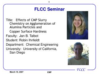
FLCC Seminar Title: Dopant and Self-Diffusion in Silicon, Germanium and Silicon-Germanium Faculty: E. E. Haller GSRA: Chris Liao Department: MS&E University: UC Berkeley FLCC Seminar
Dopant and Self-Diffusion in Silicon, Germanium and Silicon-Germanium Eugene E. Haller and Chris Liao Materials Science and Engineering, UC Berkeley Materials Sciences Division, LBNL FLCC Seminar 12/4/06
Outline • Motivation • Background • Fick’s Laws • Diffusion Mechanisms • Non-equilibrium effects • Experimental Techniques for Solid State Diffusion • Isotopically enriched structure • SIMS and Spreading Resistance Profiling • Diffusion in Si • Diffusion in Ge • Diffusion in SiGe • Conclusions and Future Work FLCC Seminar
Motivation • Why is diffusion important for feature level control of device processing? • Nanometer size feature control: - any extraneous diffusion of dopant atoms may result in device performance degradation • Drain extension Xj < 10 nm by 2008* • Extension lateral abruptness < 3 nm/decade by 2008* • Accurate models of diffusion are required for dimensional control on the nanometer scale *International Technology Roadmap for Semiconductors, 2004 Update FLCC Seminar
Semiconductor Technology Roadmap (International Technology Roadmap for Semiconductors, 2005) Difficult Challenges Modeling and Simulation FLCC Seminar
Jin Jout dx Example: Vacancy Mechanism Fick’s Laws (1855) Fick’s 1st Law: Flux of atoms 2nd Law Diffusion equations do not take into account interactions with defects! Jout Jin -RS +GS FLCC Seminar
Analytical Solutions to Fick’s Equations D = constant - Finite source of diffusing species: Solution: Gaussian - Infinite source of diffusing species: Solution: Complementary error function FLCC Seminar
Solutions to Fick’s Equations (cont.) D = f (C) Diffusion coefficient as a function of concentration Concentration dependence can generate various profile shapes and penetration depths FLCC Seminar
Direct Diffusion Mechanisms in Crystalline Solids (no native defects required) Pure interstitial Elements in Si: Li, H, 3d transition metals Direct exchange No experimental evidence High activation energy → unlikely FLCC Seminar
Vacancy-assisted Diffusion Mechanisms (native defects required) Vacancy mechanism (Sb in Si) Dissociative mechanism (Cu in Ge) FLCC Seminar
Interstitial-assisted Diffusion Mechanisms (native defects required) Interstitialcy mechanism (P in Si) Kick-out mechanism (B in Si) FLCC Seminar
Why are Diffusion Mechanisms Important? • Device processing can create non-equilibrium native defect concentrations; for Si devices: • Implantation: excess interstitials • Oxidation: excess interstitials • Nitridation: excess vacancies • High doping: Fermi level shift • The non-equilibrium defects can lead to enhanced or retarded diffusion (Transient Enhanced Diffusion) FLCC Seminar
Oxidation Effects on Diffusion • Oxidation of Si surface causes injection of interstitials into Si bulk • Increase in interstitial concentration causes enhanced diffusion of B, As, but retarded Sb diffusion • Nitridation (vacancy injection) causes retarded B, P diffusion, enhanced Sb diffusion Oxidation during device processing can lead to non-equilibrium diffusion (Fahey, et al., Rev. Mod. Phys. 61 289 (1989).) FLCC Seminar
Implantation Effects on Diffusion Transient Enhanced Diffusion (TED) -Eaglesham, et al., Appl. Phys. Lett.65(18) 2305 (1994). • Implantation damage generates excess interstitials • Enhance the diffusion of dopants diffusing via interstitially-assisted mechanisms • Transient effect - defect concentrations return to equilibrium values • TED can be reduced by implantation into an amorphous layer or by carbon incorporation into Si surface layer • Substitutional carbon acts as an interstitial sink • Stolk, et al., Appl. Phys. Lett.66 1371 (1995) FLCC Seminar
Ec 0.11 eV V--/- 0.57 eV V-/o 0.35 eV Io/+ 0.13 eV V+/++ 0.05 eV Vo/+ Ev Doping Effects on Diffusion Heavily doped semiconductors - extrinsic at diffusion temperatures • Fermi level moves from mid-gap to near conduction (n-type) or valence (p-type) band. • Fermi level shift changes the formation enthalpy, HF, of the charged native defect • Increase of CI,V affects Si self-diffusion and dopant diffusion V states (review by Watkins, 1986) FLCC Seminar
Experimental Techniques for Diffusion Introduction of Diffusion Source • Diffusion from surface • Ion implantation • Sputter deposition • Buried layer (grown by MBE) Annealing Analysis of the Profile • Radioactivity (sectioning) • SIMS • Neutron Activation Analysis • Spreading resistance • Electro-Chemical C/Voltage Modeling of the Profile • Analytical fit • Coupled differential eq. FLCC Seminar
Primary Experimental Approaches • Radiotracer Diffusion • Implantation or diffusion from surface • Mechanical sectioning • Radioactivity analysis • Stable Isotope Multilayers – new approach • Diffusion from buried enriched isotope layer • Secondary Ion Mass Spectrometry (SIMS) • Dopant and self-diffusion FLCC Seminar
a-Si cap nat. Si 28Si enriched FZ Si substrate Stable Isotope Multilayers • Diffusion using stable isotope structures allows for simultaneous measurements of self- and dopant diffusion • No half-life issues • Ion beam sputtering rather than mechanical sectioning • Mass spectrometry rather than radioactivity measurement 30Si 75As FLCC Seminar
Diffusion Parameters found via Stable Isotope Heterostructures • Charge states of dopant and native defects during diffusion • Contributions of native defects to self-diffusion • Enhancement of extrinsic dopant and self-diffusion • Mechanisms which mediate self- and dopant diffusion FLCC Seminar
Ion gun Mass spectrometer Ion detector Secondary Ion Mass Spectrometry • Incident ion beam sputters sample surface - Cs+, O+ • Beam energy: ~1 kV • Secondary ions ejected from surface (~10 eV) are mass analyzed using mass spectrometer • Detection limit: ~1012 - 1016 cm-3 • Depth profile - ion detector counts vs. time • Depth resolution: 2 - 30 nm FLCC Seminar
RSR→ → n Cuttriss ´61 (in Sze & Irvin ’68) Spreading Resistance Profiling FLCC Seminar
Si Self-Diffusion • Enriched layer of 28Si epitaxially grown on natural Si • Diffusion of 30Si monitored via SIMS from the natural substrate into the enriched cap (depleted of 30Si) • 855 ºC < T < 1388 ºC • Previous work limited to short times and high T due to radiotracers • Accurate value of self-diffusion coefficient over wide temperature range: 1153 ºC, 19.5 hrs 1095 ºC, 54.5 hrs (Bracht, et al., PRL 81 1998) FLCC Seminar
ni Interstitialcy mechanism Vacancy mechanism Si and Dopant Diffusion Arsenic doped sample annealed 950 ˚C for 122 hrs extrinsic intrinsic Io I- I-- FLCC Seminar
ni Interstitialcy mechanism Vacancy mechanism Si and Dopant Diffusion Arsenic doped sample annealed 950 ˚C for 122 hrs IoI-I-- FLCC Seminar
ni Interstitialcy mechanism Vacancy mechanism Si and Dopant Diffusion Arsenic doped sample annealed 950 ˚C for 122 hrs IoI-I-- FLCC Seminar
Si and Dopant Diffusion FLCC Seminar
f C D = + + = - - - I I I D ( n ) f C D f C D D ( n ) o o o + + + Si i tot Si i I I I I I I Native Defect Contributions to Si Diffusion (Bracht, et al., 1998) Diffusion coefficients of individual components add up accurately: (B diffusion) (B, P diffusion) (As, P diffusion) FLCC Seminar
Germanium Reenters Device Technology • Diffusion in Ge (self- and dopant diffusion) • Diffusion in Si stressed by Ge • Diffusion in SiGe alloys • SiGe isotope superlattices FLCC Seminar
Diffusion in Ge Self-Diffusion Annealed 586 °C for 55.55 hours Ge self-diffusion coefficient determined from 74Ge/70Ge isotope structure Fuchs, et al., Phys. Rev B51 16817 (1995) FLCC Seminar
Si Diffusion in Ge Annealed at 550 °C for 30 days H. H. Silvestri, H. Bracht, J. L. Hansen, A. N. Larsen, and E. E. Haller, "Diffusion of silicon in crystalline germanium," Semiconductor Science and Technology, vol. 21, pp. 758-62, 2006. FLCC Seminar
1954 1967 2004 Uppal et al., JAP 96, 1376. (2004). B Diffusion in Ge • Diffusion data for Boron in Ge are very limited • Activation energy is very high for B diffusion in Ge • Non-equilibrium transient effects appear to be small FLCC Seminar
As Diffusion in Ge • As diffuses by vacancy mechanism • Diffuses as singly negatively charged As-V pair erfc fit intrinsic regime: concentration independent diffusion H. Bracht and S. Brotzmann, Materials Science in Semiconductor Processing In Press, Corrected Proof, 2006. FLCC Seminar
Self- and Dopant Diffusion in Ge H. Bracht and S. Brotzmann, Materials Science in Semiconductor Processing In Press, Corrected Proof, 2006. FLCC Seminar
Effect of Strain on Diffusion in Si P. R. Chidambaram, et al. IEEE Transactions on Electron Devices, vol. 53, pp. 944-64, 2006. Tensile Compressive FLCC Seminar
Simultaneous Si and Ge Self-Diffusion in Si1-xGex x = 0.05 x = 0.25 T = 1100 °C ; t = 30 min T = 1050 °C ; t = 45min 28Si70Ge 28Si70Ge FLCC Seminar
x = 0.05 x = 0.25 Si and Ge Self-Diffusion in Si1-xGex H. Bracht et al. unpublished, 2006 A. Strohm, et al. Physica B, vol. 308-310, pp. 542-545, 2001 FLCC Seminar
900ºC P. R. Chidambaram, et al. IEEE Transactions on Electron Devices, vol. 53, pp. 944-64, 2006. Dopant Diffusion in Si1-xGex (1996) (2001) (2003) (2001) (2003) FLCC Seminar
B Diffusion in Si1-xGex • Boron diffusivity in strained as well as relaxed SiGe alloys decreases with increasing Ge content • Unique among common group III or V dopants in SiGe • Lever et al. suggest the formation of Ge-B pairs to explain the retardation • Wang et al. and Delugas and Fiorentini report an increase in migration energy with increasing Ge content due to local strain • True retardation mechanism still debatable P. R. Chidambaram, et al. IEEE Transactions on Electron Devices, vol. 53, pp. 944-64, 2006. and references therein FLCC Seminar
As Diffusion in Si1-xGex P. Laitinen, et al. Physical Review B-Condensed Matter, vol. 68, pp. 155209-1-6, 2003 FLCC Seminar
Conclusions • Diffusion in semiconductors is increasingly important to device design as feature level size decreases. • Self-diffusion coefficients and dopant diffusivities can be relatively easily obtained in Si, Ge, and SiGe, however, diffusion mechanisms are largely unknown. • Diffusion using stable isotope multilayer structures will yield important diffusion parameters and diffusion mechanisms. • The fundamental understanding of diffusion mechanisms will greatly help the device processing modeling and simulation FLCC Seminar
nat. Si1-xGex 28Si1-x70Gex nat. Si1-xGex SiGe graded buffer layer Si substrate Future Work • Use SiGe isotope multilayer structures to study simultaneous self- and intrinsic dopant diffusion • Determine not only the diffusivities, but also the diffusion mechanisms • Effect of strain will be studied by varying nat SiGe composition x = 0.05 FLCC Seminar
amorphous Si cap 100 nm 28Si1-x70Gex 100 nm nat. Si1-xGex SiGe graded buffer layer Si substrate Future WorkSi1-xGex Multilayer Structures • Five alternating 28Si1-x70Gex and natural Si1-xGex layers with amorphous cap • Implant dopants (B, P, As) into amorphous cap • Simultaneous Si and Ge self-diffusion and dopant diffusion with intrinsic and extrinsic dopant concentration Proposed isotope heterostructure: MBE grown - Group of Prof. Arne Nylandsted Larsen FLCC Seminar

