Electron Energy-Loss Spectrometry (EELS)
Electron Energy-Loss Spectrometry (EELS). Charles Lyman Lehigh University Bethlehem, PA. Based on presentations developed for Lehigh University semester courses and for the Lehigh Microscopy School. EELS in TEM/STEM. Analyze energies of electrons transmitted through the specimen

Electron Energy-Loss Spectrometry (EELS)
E N D
Presentation Transcript
Electron Energy-Loss Spectrometry (EELS) Charles Lyman Lehigh University Bethlehem, PA Based on presentations developed for Lehigh University semester courses and for the Lehigh Microscopy School
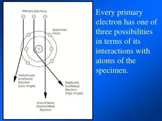
EELS in TEM/STEM • Analyze energies of electrons transmitted through the specimen • Also calledAnalytical Electron Microscopy; really AEM includes EDS, CBED, EELS, CL, Auger, etc. • Advantages: • Spatial resolution in STEM ~ d, the electron beam size • Detectability ~ 10x better than EDS • Any solid • Qualitative analysis of any element of Z > 1 • Quantitative analysis by inner-shell ionization edges of elements • Rich signal includes chemical information, etc. • Difficulties: • Need very thin specimen: t < 30 nm • Intensity weak for energy losses DE > 300 eV • L- and M- edges not very obvious for some elements from Williams and Carter, Transmission Electron Microscopy, Springer, 1996
Parallel-Collection EELS (PEELS) • Gatan PEELS • Under TEM viewing screen • Entrance aperture selects electrons • Magnetic prism disperses electrons by energy • Spectrum collected on a cooled 1024-channel diode array from Williams and Carter, Transmission Electron Microscopy, Springer, 1996
Object plane Above desk Below desk Image plane Magnetic prism “lens” Standard Instrument: Gatan PEELS from Williams and Carter, Transmission Electron Microscopy, Springer, 1996
Spectrometer Collection Semiangle b • bis the most important parameter for quantification • Semiangle subtended at the specimen by the entrance aperture of spectrometer • must know this angle • must keep constant for spectral comparisons Image Mode b is controlled by objective aperture Diffraction Mode b is controlled by EELS entrance aperture from Williams and Carter, Transmission Electron Microscopy, Springer, 1996
Energy Resolution • Energy resolution is limited by the probe-energy distribution and spectrometer resolution • Probe energy resolution (depends on gun current) • W: 2-3 eV • LaB6: >1 eV • Warm FEG: 0.55-0.9 eV • Cold W FEG: 0.25-0.5 eV • Monochromated FEG: • 0.01 eV demonstrated • 0.1-0.3 eV typical use • Approximately Gaussian zero-loss peak Measure as width of the zero-loss peak Zero-Loss Peak 200keV / 150pA Cold-FEG 0.37eV @FWHM Field-emission distribution Data courtesy J. Hunt
The Two EELS Modes • Image Mode • Energy Resolution • Without objective aperture, collect everything => ~ 100 mrad • Energy resolution is controlled by spectrometer entrance aperture (energy resolution is not compromised) • Spatial Selection • Position analysis area on optic axis, lift screen • Area selected is effective aperture size demagnified back to the specimen plane • Spatial resolution poor (10-30 nm) • Diffraction Mode • Energy Resolution • Control b with spectrometer entrance aperture • Large aperture (high intensity) will degrade energy resolution • Small aperture (high energy resolution) will degrade signal intensity • Spatial Selection • Select area with STEM beam • Area selected is function of beam size and beam spreading • < 1 nm in FEG STEM at 0.5 nA • ~ 10 nm in W electron gun at 0.5 nA • Best for high spatial resolution microanalysis
Three Spectral Regions • Zero-loss peak • No useful info, except FWHM • Super-intense • Low-loss region • 0-50 eV loss • Plasmons • Inter/intra band transition • Inner-shell ionizations • 30 eV loss and higher • Microanalysis • Very low intensity • Usually set energy range to 1000 eV loss from Williams and Carter, Transmission Electron Microscopy, Springer, 1996
Zero-Loss Peak • Elastically scattered electrons • Collected from either 000 or hkl • Measure energy energy resolution and energy spread of gun • ~0.3-0.7 eV at best • Very intense • can overload and damage photodiode array Zero-loss peak from Ahn et al., EELS Atlas, Gatan and ASU HREM Facility, 1983
Low-Loss Region: Plasmons • Collective oscillations of weakly bound electrons • Most prominent in free-electron metals • Analysis • Energy loss sensitive to changes in free-electron density • Microanalysis of Al and Mg alloys • Thickness measurements • Plasmon mean-free-path, lp ~100 nm • Multiple peaks for thick specimens from Williams and Carter, Transmission Electron Microscopy, Springer, 1996
Thickness Measurements • Log ratio method l is total mean free path for all scattering • IT is area under entire spectrum • Io is area under zero-loss • Subtract background first for best accuracy • Rough estimate of l: • l ~ 0.8Eo nm • so for 100-keV electons • l is 80-120 nm various materials Very thin specimens: t = lp(Ip/Io) from Williams and Carter, Transmission Electron Microscopy, Springer, 1996
Inner-Shell Ionization Losses • Inner-shell electron ejected by beam electron • We measure energy loss in beam electron after event • Ionization event occurs before emission of either x-ray or Auger electron emitted • Get EELS signal regardless • Can observe “edges” for all inner-shell electrons • K-shell electron (1s) • L-shell electron (2s or L1) (2p or L2 , L3) from Spence, in High Resolution Electron Microscopy, Buseck et al. (eds.),Oxford, 1987
Energy Levels and Energy-Loss Spectrum from Williams and Carter, Transmission Electron Microscopy, Springer, 1996
Chart of Possible EELS Edges from the Gatan EELS Atlas from Ahn et al., EELS Atlas, Gatan and ASU HREM Facility, 1983
Ec Edge Energy - Edge Shape • K-edge • Ideal triangular “saw tooth” sitting on background • Intensity decreases beyond edge • Less chance of ionization above Ec since cross section decreases with increasing E from Williams and Carter, Transmission Electron Microscopy, Springer, 1996
White lines L-Series Edges and White Lines • Each element has characteristic edge energy • Sharp white lines are present when d-band unfilled from Williams and Carter, Transmission Electron Microscopy, Springer, 1996
Edge Fine Structure • ELNES - electron loss near edge structure • Sensitive to chemical bonding effects • To ~ 50 eV beyond edge • EXELFS - extended energy-loss fine structure • Analogous to EXAFS • Sensitive to atomic nearest neighbors • Located beyond 50 eV for several hundred eV from Williams and Carter, Transmission Electron Microscopy, Springer, 1996
ELNES N in boron nitride N2 in air from the Gatan EELS Atlas Note significant detail near the on-set of the edge. ELNES detail is specific to the bonding environment. from Ahn et al., TEELS Atlas, Gatan and ASU HREM Facility, 1983
Carbon ELNES Carbon K-edges of minerals containing the carbonate anion compared with three forms of pure carbon from Garvie, Craven, and Brydson, American Mineralogist, 79, (1984) 411-425
Al L2,3 Crysoberyl Rhodizite Calculation for Al octahedrally coordinated to O Tetrahedral vs. Octahedral Si L2,3 from Garvie, Craven, and Brydson (1984) from Brydson (1989)
Fe L2,3 Edge in Minerals • Chemical shift • Shape change Almandine Hedenbergite Hercynite Fe “orthoclase” Brownmillerite andradite Van Aken and Liebscher, Phys Chem Minerals 29 (2002) 188-200
Oxidation State • L3/L2 ratiosa • Fe 3.8±0.3 • FeO 4.6 • Fe3O4 5.2 • g-Fe2O3 5.8 • a-Fe2O3 6.5 • Chemical shiftb • Fe –> FeO 1.4±0.2 eV (depends on peak stripping method) from Colliex et al. (1991) Colliex et al., Phys. Rev. B 44 (1991) 11,402-11,411 Leapman et al. Phys. Rev. B 26 (1982) 614-635
60 eV - EDS cannot resolve Qualitative Microanalysis • Discrimination of TiC and TiN in alloy steel • Aluminum extraction replica from Williams and Carter, Transmission Electron Microscopy, Springer, 1996
EELS Quantification • Single scattering in a very thin specimen assumed • For each element assume: PK = the probability for ionization sK = the ionization cross section N = number of atoms per unit area See Egerton, Electron Energy-Loss Spectroscopy in the Electron Microscope, Springer, 1996
Extracted edge intensity Low-loss intensity ~ IT Fitted background EELS Quant Procedure • Collect spectrum with known collection angle bfrom a very thin specimen region • Calculate (Ib = A E-r over d = 20-50 eV) and remove background under edge • Integrate edge intensity for a certain energy window D • Determine sensitivitiy factor called the “partial ionization cross section” Courtesy J. Hunt
Microanalysis Example Courtesy J. Hunt
Specimen Thicknesss Requirement • Microanalysis requires a very thin specimen • Estimate by: • Estimate thickness using: • Assuming lp ~ 100 nm: t ≈ lp(Ip/Io) for very thin only t ~ 10 nm for microanalysis from Williams and Carter, Transmission Electron Microscopy, Springer, 1996
If Plural Scattering Occurs… Deconvolute to get this For quantitation of the ionization edge we need a true single scattering distribution Plural scattering removed by a deconvolution procedure from Williams and Carter, Transmission Electron Microscopy, Springer, 1996
Spatial Resolution • EELS not affected by beam spreading like XEDS • Only electrons within 2b are collected • STEM mode • Beam size governs spatial resolution • TEM mode • Selection apertures govern spatial resolution • Lens aberrations will limit • Delocalization • Ionization by a “nearby” fast electron • Small effect: 2-5 nm EELS ionization loss spectra have been obtained from single columns of atoms from Williams and Carter, Transmission Electron Microscopy, Springer, 1996
La M4,5 edges Atomic Resolution EELS Analysis(S. Pennycook Group, ORNL) Atomic-resolution Z-contrast STEM image of CaTiO3 doped with La La M4,5 edges only observed in spectrum collected directly from bright spot in image: single-atom resolution M. Varela et al, Phys. Rev. Lett. 92 (2004) 095502
Strategy for Analysis of Unknown Phases • Start with light microscopy, SEM, powder x-ray diffraction (XRD), the library • Straightforward interpretation (usually helps TEM analysis) • Less expensive • Far more time may be needed to prepare a suitable thin specimen • Use at least two analysis methods • EDS and CBED (powerful when used together) • Determine the elements present (EDS) • Determine the phases present (CBED) • All electron transparent specimens • Keep the ICDD PDF handy to identify d-values • EELS and HREM (structure images) • Determine the elements present (EELS) • Obtain d-values of the phases (HREM) • Only very thin specimens
Summary What Can We Get from EELS? • Microanalysis by ionization-loss edges • Light element analysis complements XES • Specimen thickness measurements • Complements XES when absorption correction needed • Bonding information from near-edge fine structure (ELNES) • Fingerprints of edge shape • Reveal metal oxides, sulfides, carbides, nitrides, etc. • Chemical shifts • L3/L2 ratio can reveal a change in oxidation state • Use known standards for comparison, e.g., Fe, FeO, Fe2O3, Fe304 • Interatomic distances from extended energy-loss fine structure (EXELFS) • Information similar to EXAFS, but from nano-sized region rather than the bulk