Euler Graph for Optimized Stick Layout in Graph Theory
Learn how to apply Euler graph to draw optimal stick diagrams for circuit layout, ensuring efficient design and functionality. Start with PDN and PUN vertex placement, Euler paths, and Poly optimal ordering.


Euler Graph for Optimized Stick Layout in Graph Theory
E N D
Presentation Transcript
Euler Graph Using Euler graph to draw layout
Graph Representation • Graph consists of vertices and edges. • Circuit node = vertex. • Transistor = edge • Verify that graph represents PDN:
Building PUN from PDN • Place PUN vertices (empty circles) in eachconfined area in PDN • Connect PUN vertices with edges that crossthe PDN graph edges JUST ONCE
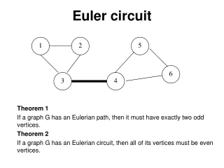
Graph Theory • Define Euler path – Uninterrupted path that traverses each edge of thegraph EXACTLY ONCE • Find Euler path in PDN graphbelow starting at x.
Optimal Input (POLY) Ordering • Common Euler path in BOTH PDN graphand PUN graph gives optimal ordering ofPOLY • What is the order of inputs for the commonEuler paths?
Two steps of stick diagram drawing Method:Stick diagrams are constructed in two steps. 1) The first step is to construct a logic graph of the schematic. A) Identify each transistor by a unique name of its gate signal (A, B, C, D, E in the example of the following Figure). B) Identify each connection to the transistor by a unique name (1,2,3,4 in the example of the Figure).
Two steps of stick diagram drawing 2) The second step is to construct one Euler path for both the Pull up and Pull down network A) Euler paths are defined by a path that traverses each node in the path, such that each edge is visited only once. B) The path is defined by the order of each transistor name. i) If the path traverses transistor A then B then C. Then the path name is {A, B, C} C) The Euler path of the Pull up network must be the same as the path of the Pull down network. D) Euler paths are not necessarily unique. F) It may be necessary to redefine the function to find a Euler path. i) F = E + (CD) + (AB) = (AB) +E + (CD)
Using Euler Graph to draw stick diagram 3) Once the Euler path is found it is time to lay out the stick diagram. A) Trace two green lines horizontally to represent the NMOS and PMOS devices. B) Trace the number of inputs (5 in this example) vertically across each green strip. These represent the gate contacts to the devices that are made of Poly. C) Surround the NMOS device in a yellow box to represent the surrounding Pwell material. D) Surround the PMOS device in a green box to represent the surrounding Nwell material. E) Trace a blue line horizontally, above and below the PMOS and NMOS lines to represent the Metal 1 of VDD and VSS. F) Label each Poly line with the Euler path label, in order from left to right. G) Place the connection labels upon the NMOS and PMOS devices. i) In the example, the connection labels are 1, 2, 3, 4. Connection 1 is the node that lies between the PMOS transistors A, B and E. The Euler path defines the transistor ordering of {A, B, E, D, C} therefore, transistor B is physically located beside transistor E. Place the connection label 1 between the transistors B and E. Later, we will route a Metal 1 connection from the drain of transistor A to the connection label of 1. ii) Connection 2 is the node that connects the PMOS transistors of E, D, and C. Since the Euler path places transistors E and D next to each other, place the connection label between these two. Later, we will route a Metal 1 strip from the source of C to connection label 2. iii) Connection label 3 lies between the NMOS transistors of A and B. iiii) Connection label 4 lies between the NMOS transistors of D and C.
H) Place the VDD, VSS and all output names upon the NMOS and PMOS devices. i) For the example of Figure there is only one output signal, called output. a) This signal is connected to the PUP device through a node located between transistors D and C. b) The signal is connected to the PDN at the node that the three transistors of A, E and D share. The Euler graph connects transistors E and D together so an output connection will be located there. Transistor A has one remaining contact that is unused, so the output label is placed at that position. ii) VDD is located upon the PMOS device at the node shared between transistors A and B. iii) VSS is located upon the NMOS device at a node that is shared between transistors B, E and C. a) The Euler path places transistors B and E together so place a VSS label between the transistors there. b) Transistor C has one remaining contact that is unused. Place a VSS label there. I) Place a blue line on the diagram to represent the output metal one material (Figure 4). Note: this line may have to be moved around depending on how the diagram connections will lay out.
4) Now its time to interconnect the device. You will probably have to experiment to find the best routing. A) Notice that Poly and Metal 1 can overlap. B) Avoid routing signals that are side by side for long lengths. This adds capacitance to the device. C) Avoid all interconnect overlap if possible. This adds capacitance to the device. D) Strive for simplicity. This will later provide the smallest and fastest devices. E) You can use Poly, Metal 2, and even Active to interconnect your device. i) Poly and especially Active adds resistance to you device. ii) Avoid using Metal 2 if possible. Metal 2 is another layer to your device that you will probably need in the next heiarchy up.
2 3 مثال 1 1
F C A F 3 1 2 VDD D B VSS مثال Euler Path: (A,B,D,C)
X=ab+cd مثال: X=?