Transistor nMOS
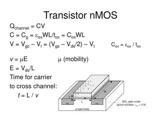
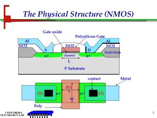
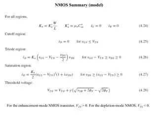
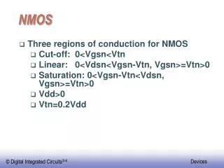
Transistor nMOS. Q channel = CV C = C g = e ox WL/t ox = C ox WL V = V gc – V t = (V gs – V ds /2) – V t v = m E m (mobility) E = V ds /L Time for carrier to cross channel: t = L / v. C ox = e ox / t ox. nMOS Linear I-V. Now we know

Transistor nMOS
E N D
Presentation Transcript
Transistor nMOS Qchannel = CV C = Cg = eoxWL/tox = CoxWL V = Vgc – Vt = (Vgs – Vds/2) – Vt v = mE m (mobility) E = Vds/L Time for carrier to cross channel: t = L / v Cox = eox / tox
nMOS Linear I-V • Now we know • How much charge Qchannel is in the channel • How much time t each carrier takes to cross
Esempio • 180 nm process • W/L= 4/2 l (360nm/180nm) • tox=40Å • m = 180 cm2/(V·s) • Vt = 0.4V = m Cox W/L = 180 * (3.9*8.85 *10-14 F/cm)/(40*10-8) =155 mA/V2 • Idsmax @ (Vgs=1V) = 155 mA/V2 *(0.6 V)2= 55 mA • Ids(Vgs=2V, Vds=1V) = 155 mA/V2 *(1.6*1) = 248 mA
CMOS Inverter substrate contact (p+) n-well contact (n+) n-well polysilicon diffusion contacts n+ diffusions polysilicon contacts p+ diffusions
DC Transfer Curve • For a given Vin: • Plot Idsn, Idsp vs. Vout • Vout must be where |currents| are equal in • Transcribe points onto Vin vs. Vout plot
Beta Ratio • If bp / bn 1, switching point will move from VDD/2
Inverter a Carico Resistivo Vout I
Inverter a Carico Attivo Vout I

