Silicon microchannels studies for the ITS upgrade
120 likes | 249 Vues
This study explores the application of silicon microchannels in electronics cooling, particularly within tracking detectors utilized in High Energy Physics (HEP). Key goals include minimizing material budget while effectively cooling large active areas under strict geometric constraints. The research highlights innovative designs, such as the “micro-bridge” concept for interconnecting silicon microchannel devices. Preliminary findings demonstrate effective thermal management with significant reduction in necessary dimensions, paving the way for future advancements in ultra-thin silicon frames. Ongoing collaboration aims to enhance the performance and integration of these cooling systems.

Silicon microchannels studies for the ITS upgrade
E N D
Presentation Transcript
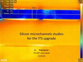
Silicon microchannels studies for the ITS upgrade Francescon ITS-MFT mini-week 12.03.14
Silicon micro-channels for electronics cooling CMOSAIC collaboration 3D Stacked Architectures with Interlayer Cooling (CMOSAIC) Agostini et al. (2008) High heat flux flow boiling in silicon microchannels • High heat transfer rate • Uniform temperature (if flow boiling) • Low mass flow rate operation • Reduced dimensions
Silicon microchannels for tracking detectors • When addressing the thermal management of the on-detector electronics fro HEP tracking detectors, the design is complicated by different constraints: • Minimization of the material budget • Cooling of large active areas • Strict geometrical and integration constraints
Silicon microchannels for tracking detectors • When designing cooling system for the tracking detectors, the design is complicated by different constraints: • Minimization of the material budget • Cooling of large active areas • Strict geometrical and integration constraints Special frame design
First prototype of silicon frame with embedded microchannels 60x15 mm2 Silicon dummy chip 100 μm thick
Results at qchip=0.3 W/cm2 The test was performed at the nominal power dissipation expected for the pixel chip. G=300 [kg·m-2·s-1] Tin=21°C Tsat=22.5°C G=750 [kg·m-2·s-1] Tin=19.5°C Tsat=21°C Dummy chip top surface with two electrodes and seven thermocouples At the nominal power dissipation expected for the pixel chip the system is able to maintain the detector surface within the thermal constraints.
Silicon microchannels for tracking detectors • When designing cooling system for the tracking detectors, the design is complicated by different constraints: • Minimization of the material budget • Cooling of large active areas • Strict geometrical and integration constraints The ˝micro-bridge˝
Interconnected silicon microchannel devices Silicon microchannel devices are limited in dimensions by the diameter of the silicon wafer used as substrate for the microfabrication. At this stage of the development, 4” wafers are used but tests on 6” wafers are on-going. However, even using 8” wafers still it would not be possible to reach the length of the ITS inner layers stave. Using larger wafers would lead to a device very hard to handle during the following integration steps. For this reason, the interconnection of several silicon microchannel devices is mandatory. In order to guarantee the interconnection of silicon microchannel devices, we developed the concept of the ˝micro-bridge˝.
Silicon microchannels for tracking detectors • When designing cooling system for the tracking detectors, the design is complicated by different constraints: • Minimization of the material budget • Cooling of large active areas • Strict geometrical and integration constraints Special fluidic design The requirement of having all the services on one side for the extraction of the ITS barrel for maintenance, forced us to develop a special fluidic path for the prototype. Inlet distribution line Micro-bridge Return line
Fabrication of the prototype The devices are fabricated in the EPFL Center of MicroNanotechology (CMi) class 100 clean room using standard microfabrication techniques.
Preliminary thermal tests: single-phase flow Test at 0.1 W/cm2 uniform power dissipation ṁ=0.4 g/s Tin=16 ᵒC
Future plans In collaboration with the Thai MicroEectronic Center (TMEC) in Bangkok, we are developing ultra-thin full silicon frames with embedded microchannels on 6˝ wafers. This will require only 2 frames for the cooling of a full IB stave. 160 μm! Before bonding 410 μm