Download
1 / 32
330 likes | 354 Vues
Explore the development of a cutting-edge 4-channel waveform sampling ASIC in 130nm CMOS for Large-Area Picosecond Photo-Detectors (LAPPD) collaboration. Discover the integration, specs, and design, along with the impressive results achieved.

E N D
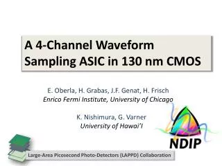
A 4-Channel Waveform Sampling ASIC in 130 nm CMOS E. Oberla, H. Grabas, J.F. Genat, H. Frisch Enrico Fermi Institute, University of Chicago K. Nishimura, G. Varner University of Hawai’I Large-Area Picosecond Photo-Detectors (LAPPD) Collaboration
LAPPD Collaboration Outline • LAPPD Detector & electronics integration overview • Waveform sampling ASIC specs & design • Results E. Oberla/JF Genat - 130nm Sampling ASIC
LAPPD Collaboration Outline • LAPPD Detector & electronics integration overview • Waveform sampling ASIC specs & design • Results E. Oberla/JF Genat - 130nm Sampling ASIC
LAPPD Collaboration The LAPPD project • Development of large-area, relatively inexpensive Micro-Channel Plate (MCP) photo-detectors • 8” x 8” phototubes = ‘tile’ • Gain >= 106 with two MCP plates • Transmission line readout – no pins! • Fast pulses + low TTS ~30ps • Large active area Photocathode MCP 1 MCP 2 Anode micro- strips (50Ω) Dual-end readout E. Oberla/JF Genat - 130nm Sampling ASIC
LAPPD Collaboration The LAPPD project • Development of large-area, relatively inexpensive Micro-Channel Plate (MCP) photo-detectors • 8” x 8” tubes = ‘tile’ • “Super Module”: • 2x3 array of 8” tiles Photocathode MCP 1 MCP 2 Anode micro- strips (50Ω) Dual-end readout Dual-end readout E. Oberla/JF Genat - 130nm Sampling ASIC
LAPPD Collaboration Detector -> Readout integration • Dual-end 50 Ω Transmission line readout – up to 2 GHz bandwidth • Waveform sampling ASICs readout both ends • High channel density • Low power • Preserve timing information • Can we push certain limitations on current waveform sampling ASICs? (i.e. sampling rate) • 130 nm CMOS 40 channel ASIC readout = ‘analog card’ E. Oberla/JF Genat - 130nm Sampling ASIC
LAPPD Collaboration Detector -> Readout integration • Dual-end 50 Ω Transmission line readout – up to 2 GHz bandwidth • Waveform sampling ASICs readout both ends • High channel density • Low power • Preserve timing information • Can we push certain limitations on current waveform sampling ASICs? (i.e. sampling rate) • 130 nm CMOS 40 channel ASIC readout = ‘analog card’ E. Oberla/JF Genat - 130nm Sampling ASIC
LAPPD Collaboration Outline • LAPPD Detector & electronics integration overview • Waveform sampling ASIC specs & design • Results PSEC-3: 4 channel waveform sampling ASIC E. Oberla/JF Genat - 130nm Sampling ASIC
PSEC-3 ASIC LAPPD Collaboration Designed to sample & digitize fast pulses (MCPs): • Sampling rate capability > 10GSa/s • Analog bandwidth > 1 GHz (challenge!) • Relatively short buffer size • Medium event-rate capability (~100 KHz) • 130 nm CMOS E. Oberla/JF Genat - 130nm Sampling ASIC
PSEC-3 architecture LAPPD Collaboration • Waveform sampling using Switched Capacitor Array (SCA) • 256 points/waveform • On-chip Wilkinson digitization up to 12 bits • Serial data readout @ 40 MHz • Region of interest readout capability • Self-triggering option Phase Compa-rator Charge pump 5-15 GSa/s Timing Generation: locked sampling w/ on chip DLL …… To 4 channel SCA’s – sample & hold E. Oberla/JF Genat - 130nm Sampling ASIC
LAPPD Collaboration PSEC-3 Evaluation Board USB 2.0 • 4 channel, 5-15 GSa/s “oscilloscope” • 5V power • Hardware trigger capability • Accompanying USB DAQ software PSEC-3 M. Bogdan- UChicago E. Oberla/JF Genat - 130nm Sampling ASIC
Sampling Rate LAPPD Collaboration • Sampling rates adjustable 2.5 – 17 GSa/s • Default setting of 10 GS/s, sampling lock with on-chip Delay-Locked Loop (DLL) Good agreement with data +post-layout simulation E. Oberla/JF Genat - 130nm Sampling ASIC
ADC performance LAPPD Collaboration • Wilkinson ADC runs successfully to 2GHz (registers can be clocked to 3GHz) • Running in 10 bit mode: • 700 ns conversion time (ramp ->0-1V) @ 1.6 GHz A/D conversion main power consumer in PSEC-3 – ~10 mW per channel (only ON during 700 ns digitization period) Test structure (counter + ring oscillator) Actual channel performance E. Oberla/JF Genat - 130nm Sampling ASIC
PSEC-3 noise LAPPD Collaboration DC level readout: Fixed pattern noise dominates -- due to cell-to-cell process variations E. Oberla/JF Genat - 130nm Sampling ASIC
PSEC-3 noise LAPPD Collaboration DC level readout: Sample noise σ ~ 1 mV Count-voltage conversion & pedestal subtraction E. Oberla/JF Genat - 130nm Sampling ASIC
Linearity & Dynamic Range LAPPD Collaboration • Dynamic range limited to ~ 1V in 130nm CMOS (rail voltage = 1.2V) • Good linearity observed Linear DC voltage scan Fit residuals + interpolation raw data linear fit Implemented in software LUT for diff. non-linearity correction E. Oberla/JF Genat - 130nm Sampling ASIC
Analog Bandwidth LAPPD Collaboration • Sine wave data – overlay 100’s of readouts: 100 MHz 600 MHz Visible attenuation along chip input at higher frequencies input much too resistive (Rin~160 Ω) fall-off due to Rin Cparasitic Sample 1 256 E. Oberla/JF Genat - 130nm Sampling ASIC
Analog Bandwidth LAPPD Collaboration • Sine wave data – overlay 100’s of readouts: 100 MHz 600 MHz -3dB Bandwidth ~ 1.4 GHz for first cells (but only ~ 300 MHz for later cells) corrected in PSEC-4 design Sample 1 256 E. Oberla/JF Genat - 130nm Sampling ASIC
LAPPD Collaboration Transmission Line-MCP readout with PSEC-3 2” x 2” Burle Planacon w/ custom PCB T-Line board laser F. Tang - UChicago PSEC-3 sampling @ 10 Gsa/s E. Oberla/JF Genat - 130nm Sampling ASIC
LAPPD Collaboration Transmission Line-MCP readout with PSEC-3 (preliminary) σt ~ 17 ps assuming nominal 100ps per cell σt ~ 13 ps after time-base calibration E. Oberla/JF Genat - 130nm Sampling ASIC
LAPPD Collaboration PSEC-3 + (upcoming) PSEC-4 PSEC-3 PSEC-4 Red= issues addressed from PSEC-3 E. Oberla/JF Genat - 130nm Sampling ASIC
PSEC-4 – 5-15 GSa/s, 1.5 GHz LAPPD Collaboration • Design targeted to fix issues with PSEC-3 • 6 identical channels • each 256 samples deep • Submitted to MOSIS 9-May 2011 • 40 parts • May get a larger run via CERN MPW if necessary E. Oberla/JF Genat - 130nm Sampling ASIC
LAPPD Collaboration Summary • PSEC-3 (soon PSEC-4) baseline ASIC for LAPPD MCP photodetectors • 80 channel DAQ system based on PSEC-3 & 4 under development • Experience with IBM 130 nm CMOS • Other applications? • Sampling rates 10-15 GSa/s achieved • analog bandwidth fixed in PSEC-4 (back from foundry ~ 9/2011) • Robust timing calibrations/measurements underway E. Oberla/JF Genat - 130nm Sampling ASIC
LAPPD Collaboration 3 National Labs +SSL, 6 Divisions at Argonne, 3 US small companies; electronics expertise at Universities of Chicago and Hawaii Goal of 3-year R&D- commercializable modules. E. Oberla/JF Genat - 130nm Sampling ASIC
LAPPD Collaboration • Questions • - Readout time: • 2 ms fixed (ADC ramp) + readout of 12-bit digital data at 40 MHz • Slide #20 (timing resolution with MCP + T-lines + PSEC3) • With how many photo-electrons ? I replied wrongly ‘one’ during the presentation, I corrected for at least 50 • (thinking 250 mV/5mV=50), still wrong… • Eric explained me later on that the MCP was quite blasted with the laser light • and there was a 10x attenuation, so the correct answer should have been 500, • I guess. NDIP 2011 -- 5 July E. Oberla/JF Genat - 130nm Sampling ASIC 25
Backup E. Oberla/JF Genat - 130nm Sampling ASIC
PSEC architecture – timing generation Phase Compa-rator Charge pump • 256 Delay units – starved current inverter chain -----------> • Sampling window strobe (8x delay) sent to each channel’s SCA • On chip phase comparator + charge pump for sample lock E. Oberla/JF Genat - 130nm Sampling ASIC
PSEC architecture -- sampling E. Oberla/JF Genat - 130nm Sampling ASIC
PSEC architecture – ADC + readout Level from sampling cell Comp. Clk enable Read enable fast 12 bit register 2-2.5 GHz Ring Oscillator 12 bit data bus Ramping circuit Readout shift register/ one-shot: “Token” … 256x … E. Oberla/JF Genat - 130nm Sampling ASIC
Bandwidth with gain=2 amplifier • Comments: • On-board amplifier (channel 4) unstable with unity gain – works with gain=2 • -3dB BW ~700 MHz for first cells • Amplifier = THS4304 E. Oberla/JF Genat - 130nm Sampling ASIC
PSEC-3 leakage • average~ 70 pA (sampling capacitance ~50 fF w/ parasitics) E. Oberla/JF Genat - 130nm Sampling ASIC
PSEC-3 pedestal temperature dependence (~-1 mV/°C) E. Oberla/JF Genat - 130nm Sampling ASIC