Download
1 / 26
260 likes | 427 Vues
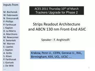
Inputs from M. Bochenek W. Dabrowski N. Dressnandt P . Phillips P. Farthouat J. Kaplon D. La Marra A. Marchioro M. Newcomer K. Swientek M. Warren E. Lipeles J. Kaplon A. Grillo S. Kilani P. Farthouat J. Goricek J. De Witt ….

E N D
Inputs from M. Bochenek W. Dabrowski N. Dressnandt P. Phillips P. Farthouat J. Kaplon D. La Marra A. Marchioro M. Newcomer K. Swientek M. Warren E. Lipeles J. Kaplon A. Grillo S. Kilani P. Farthouat J. Goricek J. De Witt … Strips Readout Architectureand ABCN 130 nm Front-End ASIC ACES 2011 Thursday 10th of March TrackersUpgrade for Phase 2 Speaker : F. Anghinolfi Krakow, Penn U., CERN, Geneva U., RAL, Birmingham, KEK, UCL, UCSC ….
To situate the project • Replacement of the existing ABCN25 (CMOS 250nm) for prototyping of Silicon strips stave/module construction • More realistic power schema (1.3V instead of 2.5V) • 256 channels (strips) instead of 128 per ASIC (material reduction) • Major Changes • L0/L1 data flow control (Track Trigger) • Fixed size Data packet format (1 or 2 cluster/packet, robust against harsh environment) F. Anghinolfi
ATLAS Strips Readout Concept (Barrel) ACES 2009 Module #1 Module #2 Module #12 Cooling In TTC, Data (& DCS) fibers Opto SC (DCS link) DCS interlock HCC HCC HCC HCC HCC HCC DCS env. IN Cooling Out SC Hybrid Service bus PS cable Barrel “short” strips stave : 12 sensors of ~ 10x10cm Sensor : 1280 strips with ~ 80 microns pitch per row 4 rows with ~ 2.5 centimeters strip length F. Anghinolfi
Short Strips Hybrid model 128 strips 128 strips 256 channels ABCN FE ASIC HCC hybrid Interface Hybrid over strips detector 1280 strips 1280 strips 1280 strips 1280 strips 1280 strips 1280 strips Connections area (Power, signals) Recent proposal : 256 channels per FE ASIC (10 ABCN per Hybrid) F. Anghinolfi
GBTX Hybrid readout through the GBT system HCC 12 HCC 6 HCC 1 E-link 1 – 80-160MHz-clk E-link 2 – RXDATA : COM E-link 3 – RXDATA : L0/L1 E-link 4 – RXDATA : R3 E-link 1 – TXDATA (80-160MHz) E-link 6 – TXDATA (80-160MHz) E-link 12 – TXDATA (80-160MHz) HCC 24 HCC 18 HCC 13 E-link 1 – 80-160MHz-clk E-link 2 – RXDATA : COM E-link 3 – RXDATA : L0/L1 E-link 4 – RXDATA : R3 E-link 13 – TXDATA E-link 18 – TXDATA 1 per hybrid E-link 24 – TXDATA E-link connections btw. 12 modules (24 Hybrids) to GBTX e-links F. Anghinolfi
Power estimates for one short strips single side stave 12 sensors 12 modules 24 Readout Hybrids 1 EOS One example for Power numbers, single-side stave with short strips. Several variants exist Readout Hybrid 340mA@1.2V 1220mA@0.9V HCC, ABCN GBT, DCS Using VDD digital at 0.9V will be reconsidered after measurements of the SEU cross-section versus VDD Stave Controller 200mA@2.5V 1130mA@0.9V F. Anghinolfi
ABCN-130 Powering Schema DC-DC options 2.4V 1.2V Analogue (45mA) DC-DC Low Vdd DC/DC 1.8V DC/DC 0.9V Digital (102mA) 2.4V 1.2V Analogue (45mA) DC-DC DC/DC DC/DC 1.2V Digital (135mA) There are discussions on placing the DC-DC converters on-chip or on a separate flip-chip F. Anghinolfi
ABCN-130 Powering Serial Power (SP) options 1.2V SP Low Vdd Analogue (45mA) LDO Shunt 0.9V Digital (102mA) 1.2V 1.2V Digital (135mA) SP Shunt 1.2V Analogue (45mA) The shunt device is distributed across FE chips, controlled by a common feedback loop F. Anghinolfi
Towards ABCN 130 implementation • The present ABCN25 realization • Elements for ABCN 130 • New features in ABCN 130 F. Anghinolfi
ABCN25 Strips Readout Asic 7.7 x 7.5 mm2 128 channels 35mA @ 2.0V Analogue 135mA @ 2.5V Digital Existing vehicle for hybrid/module/stave developments F. Anghinolfi
ABCN25 Strips Readout on Hybrids US/UK version Modules and stavelets are tested with both serial or DC/DC powering sytems(but 2.5V) GVA-KEK version F. Anghinolfi
ABCN 130nm : What is new/changed ? • 256 channels (strips) per ASIC • Dual Trigger (L0/L1) data flow control • Fixed size data packet per ASIC • Extended SEU protection (not commented here) Maintained : • Serial or DC/DC power schema compatible F. Anghinolfi
ABCN 130nm : Front-End Prototype 130nm Front-end (J. Kaplon) • Channel 22um x 700um (w/o bonding pad area) • Gain 100mV/fC • Linear range 4fC (saturation at 6fC) • Peaking time 22ns • Current consumption of the front end channel; Iinput+80uA (Iinput = 100-160uA) • Power consumption @ 1.2V : 220 – 290uW / channel • Noise estimates F. Anghinolfi
ABCN 130nm : DC/DC prototype M1 Buffer M1 (PFET) 28.2mm / 0.24μm Power Efficiency = 97% • VDD= 1.9 V • VOUT= 926 mV • IOUT = 60 mA • CX= 1000 nF • CL= 200 nF • f = 1 MHz (including all circuitry) M2 Buffer M2 (NFET) 18.0mm / 0.30μm Clock Gen M3 (NFET) 18.0mm / 0.30μm M3 Buffer Step-Down converter design M. Bochenek M4 (NFET) 6.0mm / 0.30μm M4 Buffer F. Anghinolfi
ABCN 130nm : SEU Logic prototype SEU Logic circuit RTL exists Serial Register xx-SEU (4 bits,) Fast Command decoder Serial Register yy-REGSEU (7 bits) Slow Command decoder yy-SEU (7 bits) SEU Logic part (F. Anghinolfi, K. Swientek) SPP Elements (M. Newcomer, N. Dressnandt) 2x Serial Out F. Anghinolfi
ABCN 130nm : L0/L1 Data Flow Control An early “fixed” latency L0 trigger is received by all FE Asics A fraction of the detector (10%) receives a Readout Region Request (R3) to readout hit patterns relative to one L0 At reception of an L1 trigger tagged with L0 identifier, the whole detector is readout F. Anghinolfi
ABCN 130nm : L0/L1 Data Flow Control Trigger command with L0/L1 capability L02ID L1 L02ID L01ID R32 L1 L02 L01ID L01 R31 Start R3 Module @ bits L0ID selected for readout Trailer Not fixed Latency 1 1 0 0 0 1 1 1 0 0 0 0 0 0 1 1 0 1 1 1 0 0 1 0 Geographical ID L0 Signal @Fixed Latency Geographical ID L1 rate : 40-100KHz rate L0/R3 rate : 0.4-1MHz Physically there are 2 x 80Mbits/s lines carrying the above information : L0/L1 : L0 bit sync with one phase of BC, L1 bit with the other phase of BC R3 : R3 Packets (Header + Geo address + L0ID) F. Anghinolfi
ABCN 130nm : L0/L1 data Flow Control L1 latency and Event Buffer R3 latency (3us ?) DCL ODD 128 19 Pipeline (SRAM) 256 256 L1 buffer (SRAM) 20 19 WA RA WA RA SER DCL EVEN 128 L0ID BC WAgen RAgen At BC : WA=WA+1 At L0: RA=WA-L0Lat R Event Address R Event Address R3 L1 RR Data Flow Control W W R3L0ID L1L0ID Radiation tolerant (TID &SEU) SRAM design by CERN/MicroElectronics F. Anghinolfi
ABCN 130nm : Data Packets • In previous ABCD/ABCN : Data packets are built with data from adjacent chips (data concatenation built with a time constrained token signal, data packet built by a “Master” function) • Now it is proposed “Independent Fixed size Data packets” per ABCN chip : it has impact on BW, but independent data packet carry its complete identification pattern : corruption means one packet loss only. One packet payloadhas room for one or two* hit/cluster physics data of the same event. * : still under discussion F. Anghinolfi
ABCN 130nm : Data Packets Data Packet Proposal HybID Event ERC ABCNID L0ID BCID Ty pe Preformat for 4 adjacent channels : <mean> cluster size 2.35 F. Anghinolfi
ABCN 130nm : Data Packets Transmission Data is passing in a daisy-chain formed by a group of 5 chips on the hybrid. Data is passing to the HCC and from there sent through the GBT system ABCN-Last-2 data pending ABCN-Last-1 data pending To HCC T.fifo T.fifo Xoff Xoff Xoff ABCN-Last-1 ABCN-Last ABCN-Last-2 Header Data Header Header Data Data Xoff control : no timing constraint, one FIFO and some add. Logic in each chip, readout starts from last chip of the chain F. Anghinolfi
ABCN 130nm : Data Packets Transmission Simplified model giving the number of hits distribution in a 256-channel ABCN for a 5.1034 cm-2.s-2 luminosity Distribution of the number of packets transmitted by a readout hybrid in the case a packet contains 1, 2, 3 or 4 hits for a 5.1034 cm-2.s-2luminosity (100K events). To be confirmed : only extrapolation from 128 channels case F. Anghinolfi
Hybrid Controller Chip HybridController MCC_Clk CMD_BC DLL ABC Data Clock BC/L1 phase CMD_ABC_BC ABC Cmd LCL Cmd SR / Setup DCS RO L0_L1 Service side L0_L1 Hybrid (ABCN) side R3 R3short Data I Xon/off Data Concentrator FiFo Data Loop X2 Data/CLK Encode Xon/off Data II Data Loop Hybrid @ bits DCS V(temp), V(analog) F. Anghinolfi
ABCN-130 : Projection Actually building specifications together with new functionality Analogue Front-End well under control Powering schema not fixed Digital parts adapted for Track Trigger/Data reduction Less than 1mW per channel ABCN budget New event data transmission schema Expected “readiness” 2nd semester 2012 F. Anghinolfi
Backup Slide F. Anghinolfi
130nm SEU cross section (Data from the Pixel Group) • What was tested : {Standard ARM}, {DICE}, {DICE + Triplication} • What was tested : dependence over VDD (x5-10 in the range 1-1.5V) • What (has to) should be tested : {Standard IBM}, {Standard IBM + triplication}, {DICE with IBM-like cell}, all with T3 layout now (My) Approx of Pixel SEU Test results, should be verified F. Anghinolfi