Module Enhancement: Wire Length Reduction and Wider Chip Details
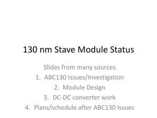
This module features a wider chip that reduces wire length by 1.1mm and increases bond pad pitch from 109mm to 119mm. Evaluations show comparisons at Liverpool M21, with brick M21 bypassed, resulting in improved HSIO with

Module Enhancement: Wire Length Reduction and Wider Chip Details
E N D
Presentation Transcript
With wider ABCn130 • Reduces wire length with same angle by 1.1 mm (6.7 to 5.6 mm)
Wider Chip Details • By widening chip by 400 mm and having only two test bond pads per row (in blue) can increase bond pad pitch from 109 mm to 119 mm
Comparisons at Liverpool M21 w/brick M21 bypassed • Our HSIO has < 200 mV peak-to-peak ripple, so might explain why it is smaller improvement • We are trying to remeasure all our modules with/without bypassing 48 V/12V converter • So far, puts noise within 10e- of expectation of capacitance • Inners: 590-615 • Outers: 600-640


![Nm]](https://cdn3.slideserve.com/6300766/slide1-dt.jpg)