Advancements in Biocompatible Electromagnetics for Embedded Medical Devices
140 likes | 273 Vues
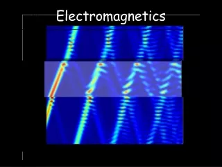
This study explores the integration of electromagnetics in biocompatible communication systems for devices and sensors embedded within the human body. It addresses critical issues such as long-term biocompatibility, mechanical and electrical safety, communication efficiency, and battery life. Key visualizations demonstrate electromagnetic energy interactions in various electronic and photonic applications. With implications for radar technology and ultrahigh-speed electronics, this research aims to advance both medical imaging and device functionality, ensuring safer and more effective healthcare solutions.

Advancements in Biocompatible Electromagnetics for Embedded Medical Devices
E N D
Presentation Transcript
Why Study Electromagnetics? Contributors: Allen Taflove Cynthia Furse
Objective • Biocompatible communication system for data up/download for devices/sensors imbedded within the body EXTERNAL DEVICE • Issues: • Long-term Biocompatibility • Mechanical Safety • Electrical Safety (SAR, shock, EMI) • Efficiency / battery life • Communication (data rate, distance, SNR, etc.)
Radar Signal Hitting Jet Fighter Plane False-color snapshot of the computed surface electric currents induced on a prototype military jet fighter plane by a radar beam at 100 MHz [A. Taflove, Computational Electrodynamics: The Finite-Difference Time-Domain Method. Norwood, MA: Artech House, 1995, pp. 11, 15, 516, 517. ]. The impinging plane wave propagates from left to right at nose-on incidence to the airplane. The surface currents re-radiate electromagnetic energy which can be detected back at the radar site.
Two sequential false-color snapshots of a microwave pulse penetrating a missile radome containing a horn antenna [A. Taflove and S. C. Hagness, Computational Electrodynamics: The Finite-Difference Time-Domain Method, 2nd ed. Norwood, MA: Artech House, 2000, pp. 9, 20, 687–690 ].
High Speed Electronics False-color visualization (bottom) illustrating the coupling and crosstalk of a high-speed logic pulse entering and leaving a microchip embedded within a conventional dual in-line integrated-circuit package (top). The fields associated with the logic pulse are not confined to the metal circuit paths and, in fact, smear out and couple to all adjacent circuit paths [Graphics courtesy of Prof. Melinda Piket-May, Dept. of Electrical and Computer Engineering, University of Colorado–Boulder, Boulder, CO. Email: mjp@boulder.colorado.edu ].
High Speed Electronics False-color visualization (bottom) illustrating the coupling and crosstalk of a high-speed logic pulse entering and leaving a microchip embedded within a conventional dual in-line integrated-circuit package (top). The fields associated with the logic pulse are not confined to the metal circuit paths and, in fact, smear out and couple to all adjacent circuit paths [Graphics courtesy of Prof. Melinda Piket-May, Dept. of Electrical and Computer Engineering, University of Colorado–Boulder, Boulder, CO. Email: mjp@boulder.colorado.edu ].
Applications in Ultrahigh-Speed Photonic Integrated Circuits Scanning electron microscope image of a portion of a prototype photonic integrated circuit [Graphic courtesy of Prof. Seng-Tiong Ho, Dept. of Electrical and Computer Engineering, Northwestern University, Evanston, IL. Email: sth@ece.northwestern.edu]. The photonic circuit is comprised of 5.0-mm-diameter AlGaAs microcavity disk resonators coupled to 0.3-mm-wide AlGaAs optical waveguides across air gaps spanning as little as 0.1 mm.
False-color visualizations illustrating the sinusoidal steady-state optical electric field distributions in a 5.0-mm-diameter GaAlAs microdisk resonator coupled to straight 0.3-mm-wide GaAlAs optical waveguides for single-frequency excitations propagating to the right in the lower waveguide [A. Taflove and S. C. Hagness, Computational Electrodynamics: The Finite-Difference Time-Domain Method, 2nd ed. Norwood, MA: Artech House, 2000 ]. Upper left—off-resonance signal; Upper right— on-resonance signal, first-order radial mode; Lower left—second-order radial-mode resonance; Lower right—third-order radial mode resonance.
Microcavity Laser Design Photonic crystal microcavity laser [O. Painter, R. K. Lee, A. Scherer, A. Yariv, J. D. O’Brien, P. D. Dapkus, and I. Kim, “Two-dimensional photonic band-gap defect mode laser,” Science, vol. 284, June 11, 1999, pp. 1819–1821.]. Top—geometry; Bottom—false-color visualization of the optical electric field distribution along a planar cut through the middle of the laser geometry.
Light Switching Light in Femtoseconds Sequential false-color snapshots of the electric field of equal-amplitude, in-phase, 100-fs optical spatial solitons co-propagating in glass [A. Taflove and S. C. Hagness, Computational Electrodynamics: The Finite-Difference Time-Domain Method, 2nd ed. Norwood, MA: Artech House, 2000, pp. 9, 20, 687–690 ]. The optical pulses propagate from left to right at the speed of light in glass. This illustrates the dynamics of a potential all-optical “AND” gate, i.e., light switching light, that could work on a time scale 1/10,000th that of existing electronic digital logic.
Imaging of the Human Body Realistic breast-tissue model derived from high-resolution magnetic resonance imaging (MRI) used to define the dielectric materials in the tumor-imaging study [Graphics courtesy of Prof. Susan Hagness, Dept. of Electrical and Computer Engineering, University of Wisconsin–Madison, Madison, WI. Email: hagness@engr.wisc.edu].
Top—MRI-derived breast model. Arrow indicates the location of the assumed actual 6-mm-diameter malignant tumor at a depth of 3 cm. Bottom—Image reconstructed from backscattered waveforms obtained by solving Maxwell’s equations [Graphics courtesy of Prof. Susan Hagness, Dept. of Electrical and Computer Engineering, University of Wisconsin–Madison, Madison, WI. Email: hagness@engr.wisc.edu].