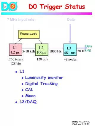
Download
1 / 15
150 likes | 280 Vues
This report details the status of the TRD pre-trigger system as presented during the TRD Status Meeting in Romania. The pre-trigger system generates wake-up signals utilizing T0, V0, and TOF detector signals. Key functionalities include generating coincidence signals, interfacing with TTC optical signals, and delivering control signals to TRD super-modules. Implementation challenges, such as timing constraints and the need for redundancy due to potential system malfunctions, are addressed. Prototyping is nearing completion with design considerations for power stability and component testing underway.

E N D
Status of TRD Pre-trigger System K. Oyama, T. Krawutschke, A. Rausch, J. Stachel, P. von Walter, R. Schicker and M. Stockmeier for the T0, V0, and TRD Collaborations Sep. 26, 2005 TRD Status Meeting in Cheile Grădiştei, Romania
The TRD Pre-trigger System • TRD pre-trigger = wakeup signal sent to TRD MCMs. • It is generated from T0, V0 and TOF detector signals using special boxes (not shoeboxes anymore). • T0: Timing detector and M.B. trigger. • V0: Vertex detection and M.B. trigger. • TOF: cosmic trigger and some physics triggers in low multiplicity environments. detailed talk by R.Schicker • Since timing is crucial, the system is placed inside L3 magnet. • The pre-trigger system should have the functionalities: • generate pre-trigger coincidence signal of T0, V0 and TOF detectors. • get TTC optical signal from CTP and insert pre-trigger into TTC stream. • provide TTC optical signals to 18 TRD super-modules. • generate control signals for FSM in MCMs (new).
Basic Concept of Implementation • To use TTCvi in the magnet is avoided because we would need VME bus and VME bus master, and TTCvi delay inside is large. CTP TTCex outside magnet L0, L1, … inside magnet bi-phase-mark decode pre-trigger system T0 bi-phase-mark encode TRD V0 (anti-) coincidence L1, L2,… + pre-trigger + FSM control TOF
The Timing Diagram of the Pre-trigger and Data Flow Interaction Time 3.5 m air 12 ns 15 ns • = 15 ns PMT response time • = 50 ns (shaping time = 120 ns) PASA T0 or V0 PMT 1 m cable 5 ns • = 25 ns delay and coincidence Front End Boxes A • = 150 ns ADC Pipeline 1 m cable CB-A CB-C 5 ns TOF FEE • = 25 ns Coincidence for Side A @ 160 ns by Eugenio 100 ns cable along z (10 m) and phi (10 m) 10 m through inner bar (7m) and radial • = 30 ns coincidence by R.Schicker 50 ns TOF Trigger Box 5 ns @ 137 ns @ 295 ns cable (would be short) • = 100 to 600 ns Programmable Delay • = 80 ns Final Coincidence and BPM encoding pretrigger for CTP 1 ns = 15 ns TTCex and TTCtx cable (40 m fiber) 200 ns @ 391ns 20 m fiber (to the farthest chamber) 100 ns @ 491ns = 50 ns coin. logic CTP inside TRD Super Module = 50 ns TTCrx 25 ns 200 ns cable (40 m fiber) • = 200 ns • = 150 ns decoding & wake-up (slow clock latch) MCM SM Filter @ 716 ns L0 @ 1015 ns Wakeup Event Buffer
Position of Pre-trigger Components inner bar (7m) A C TRD FEB FEB FEB FEB FEB FEB FEB FEB FEB FEB T0-A T0-C CB-C CB-A CB-TOF TOF signals
Front-end Box with T0 and V0 Pre-Amplifiers ~VME size side view top view to T0 and V0 rack pre-amp power T0/V0 Preamp differential signal Control 500 ps delay PECL discriminator CLK, Trig termination JTAG FPGA Independent power for pre-amp and digital part. Design is 99 % ready for prototyping. T0/V0 people are now fixing power connector for pre-amplifier, then we can produce. from detector optional for redundancy
T0 and V0 Pre-amplifier Module x10 output x1 feed-through output Design is final. 55mm x 55mm. Three SMA connectors. 0.5 W/ch. power differential output to TRD pre-trigger system input from the PMT 30 ps resolution was achieved in the test beam experiment. High ground and power stability are required. Power is given from different source with out pre-trigger system. Using inductance but still works in the B=0.5 T.
Prototype Control Board with DCS Tobias Krawutschke already started design of FPGA on the DCS.
Control Box Crates main backup 576 bits 144 cables from TOF system main backup CB-TOF (C side, with TOF trigger and TTC functionality) CB-A and CB-C
Conclusions • Prototype of control board came, and we started testing it. • Prototype design of front-end board is 99 % finished and it will be available soon. Action items: • Final space, and power requirement should be approved. • Cooling question is still open. • Radiation tests: we will have all components soon, and then just do.
Main Control Board d=210 mm DCS -delay -control -threshold TTC input (opt.) TTC F.O. 2 w=110 mm Pre-Trigger to CTP (opt. or LVD) TTC F.O. 1 DCS h=270 mm Ethernet (cat5). TTC ECL out to F.O. module (ECL) JTAG to local boxes (LVD) CLK/Control to local boxes (LVD) Triggers from local boxes (LVD) TTC F.O. can be TTCex or TTCex. DCS module is a VME size board + KIP DCS on it. DCS module has also coincidence of pre-trigger of side A and C. pre-trig to side C DCS (LVD) ptre-trig from side A DCS (LVD)
Fault Tolerance System I - System may have malfunctioning due to radiation, B field, and normal problems. - We loose entire TRD data if we loose the pre-trigger system. - We can consider to have duplication of all digital part (without analog part). Duplicated part (System II) is identical to System I and run independently. Two optical fibers should go to each TRD super-module and merged inside, it is possible (study by Marc). System II
Timing Constraint CTP must receive trigger from TRD in 6 us.