TEVATRON LONGITUDINAL PHASE DETECTION METER
TEVATRON LONGITUDINAL PHASE DETECTION METER. Aisha Ibrahim. OVERALL SYSTEM OBJECTIVE. Diagnose the energy oscillation of 36 x 36 proton and antiproton bunches as well as study transient beam loading Have observed oscillations close to cyclotron frequency prior and/or during longitudinal blowup

TEVATRON LONGITUDINAL PHASE DETECTION METER
E N D
Presentation Transcript
TEVATRON LONGITUDINAL PHASE DETECTION METER Aisha Ibrahim
OVERALL SYSTEM OBJECTIVE • Diagnose the energy oscillation of 36 x 36 proton and antiproton bunches as well as study transient beam loading • Have observed oscillations close to cyclotron frequency prior and/or during longitudinal blowup • Output modes • First mode implemented is similar to the basic capabilities of Sampled Bunch Display (SBD) • 2 parallel modes will augment module to provide • Circular Buffer : Turn by turn, Bunch by bunch data sets over 10 min • Oscillation Amplitude Detector: Output an envelope of the amplitude of the variation in phase <cadornaa@fnal.gov>
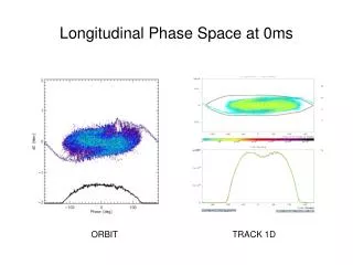
THE MATH BEHIND IT • Using the strip-line (SL) signal, the phase of the fundamental harmonic (RF freq.) of this signal respect to the RF reference can be estimated by <cadornaa@fnal.gov>
Gate Timing FPGA +/- 10 Vout 12-bit Serial DAC φi MADC ADC Clock cos Q-10bits x ADC (SIMPLIFIED) Beam pick-up (strip-line) I-10bits 2- 16MB Circular, LIFO Buffers Φ0..n x APPL. sin Gate Timing Detected LLRF VCO/VXO Clock Circuitry Ethernet Link ACNET LLRF Delayed SysClk SysClk out DDS Status Input sin cos LLRF <cadornaa@fnal.gov> MDAT TCLK AA
SINE BEAM I ANALOG PROCESSING RC Q cos RC A D C x x sin RC I RC (ELABORATED) <cadornaa@fnal.gov>
PRIMARY CHIPS / PARTS • AD8138- High Performance, High - Speed Differential Amplifier • -3 dB Bandwidth of 320 MHz, G = +1 • Fast Settling to 0.01% of 16 ns • Slew Rate 1150 V/µs • Low Input Voltage Noise of 5 nV/√Hz • 1 mV Typical Offset Voltage • AD835 - 250 MHz, Voltage Output 4-Quadrant Multiplier • Transfer Function : [(X1–X2)(Y1–Y2)/U] + Z • Very Fast: Settles to 0.1% of FS in 20 ns • High Differential Input Impedance X, Y, and Z Inputs • Low Multiplier Noise: 50 nV/√Hz <cadornaa@fnal.gov>
PRIMARY CHIPS / PARTS • AD8066 - Low-Cost High-Speed FET Input Amplifier • High speed: 145 MHz, −3 dB bandwidth (G =+1) • Low Offset Voltage 1.5 mV Max • High Common-Mode Rejection Ratio (CMRR) : -100 dB • No Phase Reversal • AD9201 - Dual Channel 20 MHz 10-Bit Resolution CMOS ADC • Differential Nonlinearity Error: 0.4 LSB • Signal-to-Noise Ratio (SNR): 57.8 dB • Effective Number of Bits (ENOB) : 9.23 • Pipeline Delay : 3 clock cycle latency (min clock period 44ns, 50% duty cycle) <cadornaa@fnal.gov>
PRIMARY CHIPS / PARTS • ALTERA Cyclones- EPC1C3T144 & EPC16Q240 • Samsung K4S561632E –TC75 • 16M x 16, 133MHz freqmax synchronous Dynamic RAM • DAC8043 -12-Bit Serial Input Multiplying CMOS D/A Converter • Low 61/2 LSB Max INL and DNL • Min clock period 240ns <cadornaa@fnal.gov>
PRIMARY CHIPS / PARTS • TI MSP430F149 • 16-Bit Ultra-Low-Power Microcontroller, 60kB+256B Flash, 2KB RAM, 12 bit ADC, 2 USARTs, HW multiplier • WIZnet iinChip W3100A-LF • Mini network module including hardwired TCP/IP chip, Ethernet PHY and other glue logics • 10/100 Base T Ethernet (Auto detection) Interface • Protocols : TCP, UDP, IP, ARP, ICMP, MAC <cadornaa@fnal.gov>
Gate Timing FPGA +/- 10 Vout 12-bit Serial DAC φi MADC ADC Clock cos Q-10bits x ADC (SIMPLIFIED) Beam pick-up (strip-line) I-10bits 2- 16MB Circular, LIFO Buffers Φ0..n x APPL. sin Gate Timing Detected LLRF VCO/VXO Clock Circuitry Ethernet Link ACNET LLRF Delayed SysClk SysClk out DDS Status Input sin cos LLRF <cadornaa@fnal.gov> MDAT TCLK AA
FPGA TIMING • Synchronization of domains • SysClk (VXO) is phase locked to LLRF • Lock the ADC clock phase to that of the LLRF • Unable to reset the PLL post scaling counters in the cyclone clock synthesizer section. • The phasing can be done with two counters, a modulo 8 for the ADCx2 clock and a modulo 14 for the RFx2. These counters are reset by the rising edge of the output of a flip-flop clocked by RF and whose data input is the 8RF/7. At the time this flip-flop changes state, the two clock trains have a consistent phase. • In the PLL, the ADCx2 clock is set to a 22.5 deg phase shift with respect to the RFx2 clock to avoid coincident edges which would cause metastability in the phase detector flip-flop. <cadornaa@fnal.gov>
FPGA TIMING • Uniquely identifying position in orbit (i.e. bunch or gap ?) is achieved with a set of counters • Same set of counters allows gate timing to be adjusted coarsely by 132nsec (x01) or finely by 10nsec (x10). <cadornaa@fnal.gov>
FPGA PHASE CALCULATION • Calculate the average over “N” cosine ADC samples for each of the 36 bunches • Calculate the average over “N” sine ADC samples for each of the 36 bunches • Calculate the average over “N” cosine-pedestal samples • Calculate the average over “N” sine-pedestal samples • Subtract pedestal samples from phase samples • Calculate sin² and cos² and compare intensity to threshold • Calculate arctan(cos/sin) using 45° lookup table • Result is a 12-bit phase in degrees • Tag bit15 in phase if intensity is less than threshold <cadornaa@fnal.gov>
Gate Timing FPGA +/- 10 Vout 12-bit Serial DAC MADC ADC Clock cos I-10bits x ADC Beam pick-up (strip-line) Q-10bits 2- 16MB Circular, LIFO Buffers x APPL. sin Gate Timing Detected LLRF VCO/VXO Clock Circuitry Ethernet Link ACNET LLRF Delayed SysClk SysClk out DDS Status Input sin cos LLRF <cadornaa@fnal.gov> MDAT TCLK AA
OUTPUT #1 : SLOWDAC • Each phase of the selected bunch is calculated every turn; then, “N” samples are averaged. • For a user-specified bunch, the resulting average phase sent to a 12-bit serial input CMOS DAC. • The DAC output is connected to a MADC channel, which has an associated ACNET device. • Assuming a 128 turn average, this gives an effective output rate of 372 KHz. Slow data Slow data I I-10bits atan(I/Q) = φi ADC Q-10bits Fast data Q <cadornaa@fnal.gov>
OUTPUT #2 : CIRCULAR BUFFERS • The longitudinal phase monitor includes an external memory bank, consisting of two 10 minutes LIFO circular buffers. • The format of the buffers consist of sequential arrays of 39 16-bit elements • an incrementing 32-bit sample count, indicating the start of the buffer • a 16-bit average phase of the following 36 data elements • the 16-bit average phase over 128 turns for each of the 36 bunches • As a result, each array is completed every 1024 Tevatron cycles and is 39 words long. All data values are scaled to 12 bit values. • Started and stopped either by a manual trigger or by a programmed TCLK event. • Once a buffer is stopped, the last MDAT timestamp is recorded. • If an “auto-restart” option is enabled, then the buffer’s arm bit will persist. en. • However, if the “auto-restart” option is not enabled, the buffer needs to be re-armed to begin collecting data again. I Slow data I-10bits atan(I/Q) = φi ADC Fast data Q-10bits Q <cadornaa@fnal.gov>
OUTPUT #3 : Oscillation Amplitude Detector • The same 39 element array is to be processed to output an “envelope” that depicted the magnitude of the phase variation for each bunch. • This processing would result in limiting the bandwidth to ½ Hz. • This output mode is still to be better defined. I Slow data I-10bits atan(I/Q) = φi ADC Q-10bits Fast data Q <cadornaa@fnal.gov>
What has been done … • Implemented “SLOWDAC” mode: 12-bit MADC output which provides the average phase of a selected bunch over 128 turns • Took measurements to show linearity when TEV in collider mode or uncoalesced mode • Implemented pedestal subtraction • Implemented TCLK & MDAT Decoders • Implemented 2 – 10 minute circular buffers • Data format: sample count, average of 36 samples, 1-36 phase averages over 128 turns (1 per bunch) • Manual & Programmable TCLK event-based start/stop/arm/auto-restart controls • Investigated θ calibration : 30-40% discrepancy • Implemented “threshold” comparison to identify non-existent bunches <cadornaa@fnal.gov>
What is next to do … • Sort out “issues” of data transfers over Ethernet/OAC • Investigating 1° noisy spots at ±45° and ±135° • Investigate output with WCM signal instead of stripline • Develop user end application • Devise test setup to “jiggle” one of 36 bunches • Oscillation Amplitude Detector • Testing and more testing… <cadornaa@fnal.gov>