Fiber Optics
Fiber Optics. Southern Methodist University EETS7320 Fall 2007 Lecture 8A Slides only. (No notes.). Electromagnetic Fields in Fiber Optics. EM field is inherently internal to the fiber core

Fiber Optics
E N D
Presentation Transcript
Fiber Optics Southern Methodist University EETS7320 Fall 2007 Lecture 8A Slides only. (No notes.)
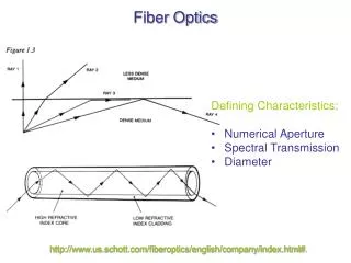
Electromagnetic Fields in Fiber Optics EM field is inherently internal to the fiber core • Total Internal Reflection occurs at boundary between two dielectric materials with different dielectric constant () values (also described as different index of refraction n) • Minimal external electromagnetic field prevents most attempts at “wire tapping” and minimizes “crosstalk” effects • Reflection also occurs at boundary between metal (copper/brass or silver plating on copper), but reflection at dielectric boundary is almost perfectly efficient • In one type of fiber (single mode) the wave power flows substantially parallel to the axis of the fiber (difficult to describe by means of geometric optics picture) • Very similar to wave propagation in hollow metal waveguides • Microwave waveguide is a hollow rectangular or elliptical cross section metal tube • Power flow vector zig-zags between walls by multiple reflection in multi-mode fibers
Major differences in signal loss • Reflection at metal surface loses ~ 1% of power, reflects 99%. 100 successive reflections leave only 36% of original power. • Reflection at a dielectric surface loses only ~ 0.00001% of power, reflects 99.99999%. 100 reflections leave 99.99900000495% of original power.
Geometric Optics Description • The ability of optical fiber to guide infra-red light (electromagnetic waves) with low power losses can be explained most easily, although only approximately, via concepts of geometric optics • The full explanation, particularly for single mode fiber, requires a wave description • The total internal reflection at the interface between high and low index glass is almost 100% power efficient, much better than metallic mirrors (silver, aluminum, etc.) • Over a million internal reflections occur in a km of multi-mode fiber, with loss of only ~0.5 dB, because each reflection is over 99.99885% efficient • metal surface reflection, at 97% efficiency, would produce 130,000 dB loss in a geometrically similar 1 km length.
Snell’s “Law” • Demonstration with glass of water no=1/co=oo :vacuum (or air) n1=1/c1=1o :lower index medium n2=1/c2=2o :higher index medium Snell’s “law”: n2•Sin(D) = n1•Sin(F) Incident ray power is partly in reflected ray, partly in refracted ray. Angle of Reflected Ray R Angle of Refraction F R=D and Sin(R)=Sin(D) Line perpendicular to interface at point where ray intersects interface. Angle of Incident Ray D Material with lower dielectric constant , faster wave speed, c1, smaller index n1. Material with higher dielectric constant , slower wave speed, c2, larger index n2.
Critical (Brewster’s) Angle Brewster’s angle B: n2•Sin(B) = n1•Sin(90º) so Sin(B)= n1/n2 Any angle DB produces total internal reflection. • Demonstration with glass of water Incident ray power is totally in reflected ray. This situation is called “total internal reflection.” Angle of Reflected Ray R Hypothetical surface wave (zero power) Angle of Refraction F= 90º Line perpendicular to interface at point where ray intersects. Angle of Incident Ray DB D “evanescent” standing wave or reflected ray described by wave theory Material with larger index n2. Material with lower index n1.
Total Internal Reflection • When angle of incidence is beyond B, ~100% of optical power is reflected internally • some sources measure angle from the perpendicular line rather than from the interface, so inequality is stated differently • When you (or a fish) go under a smooth water surface (e.g., a swimming pool), you can see up into the air only inside a circle. Outside that circle, you see only reflections from the surface. B Location of your (underwater) eye
Wave Phenomena • Wave treatment of light gives a more comprehensive explanation than geometric ray treatment • Explains evanescent wave, which travels away and back to/from interface in lower index medium, but has exponentially decreasing amplitude with distance. • Evanescent optical wave can be “recaptured” by nearby high index material. This is basis of some “non-contact” fiber light measuring instruments • Single mode fiber best explained by wave analysis • Wave propagates along central axis without geometric reflections from interface between core and cladding, • optical wave intensity at edges of core is lower because wave components are not in phase there (edge of first Fresnel zone)
Structure of Optical Fiber • Manufactured by diffusing “dopant” (alloy) chemicals into inside of a ~10 cm (outside diameter) hollow tube to modify the chemical composition, and thus modify the refractive index; • Tube is then heated and pulled. This collapses the hole in the center while the tube shrinks in diameter to a thin fiber. • Plastics are used as well as glass (but seldom for telecom fiber) by running high index plastic fiber through liquid plastic to coat it with lower index plastic cladding. • Single mode silica glass fiber today: ~ 0.1 dB/km power loss (thus up to 100 km fiber spans between repeaters) • Research on exotic glass compositions (chalcogenide glass, etc.) promises even lower loss, but other negative aspects (like large changes in n due to small temperature changes) have prevented widespread use of chalcogenide fiber. • Chalcogenide glass formulations contain some of the following elements : As, Ge, P, Sb, Ga, Al, Si, etc.
Typical Fiber Structure • Many fibers may be gathered in a protective covered cable, with steel or kevlar™ plastic “rope” (not shown) incorporated for pulling strength. Plastic protective jacket, prevents mechanical damage to outside surface of fiber. Can be removed for splicing by cutting or dissolving. Typically color coded for identification of each fiber. Lower index glass cladding typical light ray High index glass core
Multi-mode (Step-index), Graded Index, Single Mode • Cross sectional views ( should be circles*) Multi-mode Graded Index Single Mode *non-circularity of images is an artifact of computer artwork software. 125m ~80m ~10m Accurate alignment less needed for splicing. Higher loss. Major time dispersion of short optical pulses due to different geometric paths. Less used today, but historically important. Accurate alignment less needed for splicing. Higher loss. Reduced dispersion due to lower wave speed in central rays, higher wave speed (lower index) in outer part of core. Used for “last mile” and service drops, with single mode reserved for long runs. Accurate alignment needed for splicing. Best low loss. Most widely used fiber type for long spans.
Single Mode Fiber Propagation • Single mode can’t be described accurately by geometric (ray tracing) optics • Parallel flat mirror model shows essential principles of single mode fiber operation, without the complication of circular geometry • Infra-red power is focused in a narrow beam due to the combination of direct and reflected rays • radiation that would otherwise spread to the sides is cancelled due to destructive interference with reflected image radiation • Rays from side reflections are inverted in electric field polarity for each reflection • Two mirrors in the model are separated by about 10 wavelengths, similar to single mode dimensions. Image sources of alternating polarity appear to be present on both sides of the true source.
Plane Mirror Model (Wave propagation direction.) Red light-source symbols are in phase with real source. Green light-source symbols are 180º or /2 out of phase with real source. Real light source. All others are images. d= approx 6•, about 8 µm for 1300 nm Two plane mirrors represent total internal reflection surfaces of fiber core. True length of mirrors in propagation direction is actually very long. “back” side of this Mirror is drawn in black. Distant “graph paper”shows brightness (power intensity) vs. distance off the center line of single mode fiber. Most of the power is concentrated in the center. Off-center power is smaller due to destructive interference between “real” light sources and Reflected image light sources. Center line of fiber
Mode Descriptions • Single mode power density is almost uniform across the ~8 µm core diameter • The major power flow is directly along the center axis • Multi-mode or graded index fiber supports an optical “ray” that actually has less than 8 µm diameter. This ray can only propagate by reflecting diagonally from side to side of the 80-100 µm diameter core • The larger diameter of the core produces a “tighter” internal optical beam • To launch the beam diagonally into the core, the phase angle of the entering beam is intentionally different at different points across the diameter. • This situation is an example of the production of a narrower beam from a wider array of radiating sources. • So-called “smart antennas” or “adaptive beam forming” in cellular base stations make use of the same principle
Infra-red Electro-Optic Converters • Semiconductor light emitting diodes (LEDs) normally produce electro-magnetic radiation from electrons as they cross the diode junction during forward current conduction. • The change in the electron energy is proportional to the frequency of the light emitted: E=h•frequency. • Optical power (brightness) is proportional to electric current. • The energy change (“color”) can be controlled by the type and amount of alloy materials used on the P and N sides of the diode junction. Different materials have distinct energy differences between energy levels at which the electrons may “stay.” • The wavelength of the light produced is inversely proportional to the frequency f (or to the energy change) • Change in electron energy E= h•f = hc/, where wavelength =c/f • Wavelength in optical region of spectrum now usually measured in nanometers. 1 nm=10-9 m. • Older unit of wavelength, Ångstrom: Å=10-10 m (=0.1 nm) • Planck’s constant: • h=6.625•10-34 W•s2 • (or joule•sec) • speed of light: c=3•108 m/s
Wavelength and “Color” Names Ultra-violet* * UV, IR not visible to human eyes Infra-red* blue green red • Wavelength (and “color”) can be controlled by type and amount of “dopants” (alloy materials) used to make the P and N sides of the light emitting diode. • LEDs with infra-red output used as electro-optic (EO) converters for step or graded index fibers • Light emitting diodes (LEDs) with visible light output are also used for indicator lights, etc. • Construction of two parallel semi-reflecting surfaces on the diode with proper spacing relative to desired wavelength produces enhancement of one wavelength, yielding almost monochromatic LASER radiation (laser diode -- LD), used for single-mode fiber • Proper efficient coupling of light into the fiber core is a major design consideration as well (not discussed here) 400nm 500nm 600nm 700nm 850nm 1300nm 1550nm 850, 1300 and 1550 nm are local loss minima in the fiber transmission spectrum. These wavelengths often used for fiber systems.
Wavelength Refers to “in-Air” Measurements • Wavelength of the same “color” optical signal is shorter inside glass or plastic • This is the result of slower wave speed in glass or plastic (compared to air or vacuum) • The frequency (cycles per second or Hz) of the wave is the same in air or in glass or plastic • For a solid with index of refraction 1.3, the wavelength of a wave is 30% longer in air • Measurements of wavelength are typically made in air
Infra-red Detectors • A reverse-biased (negative voltage on the anode electrode) semiconductor diode has a normally very small so-called “leakage” current that increases due to higher temperature or due to illumination of the junction with light of appropriate wavelength • Electric current only occurs when “conduction” electrons, which are moveable, are present in the junction region • Light transfers energy to relatively immovable valence band electrons, causing them to change their electronic energy level (and their wavelength) so that they can move through the atomic lattice in the conduction band range of energy levels • Photovoltaic cells are large flat junctions optimized for sunlight (solar power cells) • Photodetectors for fiber are small and optimized for infra-red • Frequency of detected light must be higher than Evc/h, where Evc is the energy change between valence and conduction band energy levels. Light at lower frequencies (longer wavelengths) produces no conduction band electrons and thus no signal-related current • Amount (in mA or µA) of signal current is proportional to the brightness (power level) of the light (and to the number of moving electrons per second)
Avalanche Photo-Diodes (APD) Detectors • For higher sensitivity to very low light power levels, avalanche photo-diodes are used • High dopant concentrations and large negative power supply voltage produce a high electric field strength in the center region of the semiconductor junction of an APD. • This produces high acceleration of conduction electrons when such electrons are “produced” by radiation absorption, giving these electrons high kinetic energy. • High kinetic energy electrons strike other valence electrons, transferring energy to them and thus producing more conduction band electrons • This is a chain reaction, like a rock slide avalanche on a mountainside! It produces multiple conduction electrons per light photon, rather than only one electron per photon • The result is much higher current for a low light brightness • Unfortunately also more “dark current” due to thermally produced conduction band electrons • APDs are the mainly used with long fiber spans, single mode fiber applications
Preferred Infra-red Wavelengths • 850 nm wavelength (short-haul LEDs) • 1300 nm wavelength • 1550 nm wavelength • Each is a local minimum of glass transmission loss (see graph of loss vs. wavelength in Bellamy, p. 385 or other sources) or was a convenient wavelength in terms of historically available LED technology (850 nm in 1970s, 1980s) • Higher absorption at intermediate wavelengths is due to atomic and molecular vibration resonances in the silica fiber • Some combinations of atoms (OH “hydroxyl” ion pairs, etc.) oscillate, absorbing and re-radiating (scattering) IR light in all directions
Fiber Optic Transmission • Electro-Optic (EO) Converter • Light emitting Diode (LED): lower bit rates • Laser Diode (LD): higher bit rates, used for long hauls*, nearly monochromatic optical spectrum • Opto-electric (OE) Detector • Photo Detector Diode:short hauls* • Avalanche Photo Diode: better sensitivity, long hauls* • Binary Transmission Coding: On-Off • Single wavelength data rates over 1.6 Gb/s are feasible with single mode fiber, but requires higher electric power, more costly electronic components. • So-called wavelength division multiplexing (WDM) increases total data rate by transmitting two or more independent bit streams on different optical wavelengths (different “colors”). • Different wavelength optical signals (at or near 1300 and 1550 nm) can be transmitted simultaneously, separated at detectors by appropriate filters. Filters cause additional optical power loss. Practical WDM systems mostly use erbium doped fiber amplification (EDFA– laser amplification) *Long/short “haul” refers to source-to-detector distance.
Optical Repeaters • In general, optical repeaters perform functions similar to electrical digital repeaters: the “Three Rs”: • Regenerate (amplify, compensate for power loss) • Reshape (correct pulse wave-shape for distortions due to time dispersion) • Retime (correct for jitter) • OEO Repeaters • Historical optical repeaters use an OE detector, electrical amplification and pulse shaping, and a EO LED or LD to transmit the repeated pulse stream into the next span. • Only one wavelength can be processed by a single OEO repeater. • Many optical and electronic components and some manual adjustment at installation time are required. This is a relatively complicated and costly device. • A simpler type of all-optical repeater, particularly one that amplifies all the infrared wavelengths that are present, is desirable
EDFA: Direct Optical Amplification Erbium-doped fiber amplifier (EDFA) is an Infra-Red LASER (Light Amplification by Stimulated Emission of Radiation) which converts shorter wavelength IR source (“pump”) power into greater power at signal wavelength(s). • Advantages: • Simpler, uses less components than electro-optics, particularly for multiple wavelengths on same fiber (WDM) • Amplifies many different optical wavelength signals present in WDM (present and future as well) • Compensates for optical losses due to filters and optical combiners used in WDM • But… optical amplification does not correct timing or wave shape (two of the “3 Rs”)
LASER Amplification • Individual lower energy electrons absorb light wave energy and change their spatial electric charge configuration (they “move” to a higher energy level) at random time intervals • Individual higher energy level electrons radiate light wave energy at random time intervals. When light waves are present at a frequency corresponding to the normal radiation frequency (f=E/h) for that downward energy change, the number of electrons that randomly radiate per unit time is increased. This increase is called “stimulated emission.” • To continue amplifying, there must be a ready supply of high energy electrons. Electrons are continuously “pumped” up from a still lower energy level to the high energy level by constant irradiation using a much higher frequency, shorter wavelength optical source. • Arthur L. Schawlow (1921-1999) and Charles H. Townes first built an amplifier using stimulated emission for amplifying microwaves. Gordon Gould is also credited with theoretical invention of the LASER in the patent office. Same method later applied to visible and infra-red light. Schawlow and Townes received Nobel prize with others. Terminology: MASER (Microwave Amplification via Stimulated Emission of Radiation) LASER (Light Amplification via Stimulated Emission of Radiation)
Why Erbium? E3 Radiation • Erbium atoms have three important energy levels. The top two levels differ by an energy difference E= E3-E2 corresponding to ~1300 nm wavelength, the desired wavelength of the amplified signal. The lowest of the three energy levels differs from the top energy level (E3-E1 ) by an amount corresponding to the “pump”signal wavelength. • A section of glass fiber made with Erbium doping is spliced into the signal-carrying fiber. This Erbium section is continuously illuminated with a “pump” optical signal of wavelength corresponding to E3-E1 • Radiative energy level transitions occur from level E3 down to E2 in proportion to the incoming (signal) light power level. The outgoing light power level is stronger. • Electrons eventually fall in energy from level E2 back to E1 as well, but produce light of a different wavelength than the 1300 nm wavelength used for optical signals. These other wavelengths are eventually absorbed by “colored” filters that only substantially pass 1300 nm infra red light. E2 E1 Pump Action (sche- Matic)
Future Possibility: Coherent Detectors • Present fiber power detectors respond with current proportional to instantaneous optical power (brightness) • No such thing as “negative brightness” • Sophisticated modulation methods (used for audio/radio frequencies) are not feasible today • So-called “phase sensitive detection” would permit discrimination between positive (in phase) and negative (180 degree or out of phase) wave amplitude, both of which have the same power level. • This would permit phase modulation, QAM, other highly efficient modulation methods which transmit many bits per symbol, as are used for modems, radio systems, etc. • For a pure sine wave, combination with a locally generated sine wave before photo-detection produces greater sensitivity, opens the possibility of phase modulation, etc.. • Requires ability to precisely control the phase of a local optical source at the detector -- very difficult to achieve!