
SlideServe
Menu
Préférences
© SlideServe · v2026

Adaptive Mirror Control System

bruce-wade avatar
17 diapositives · 385 Views · Oct 31, 2014

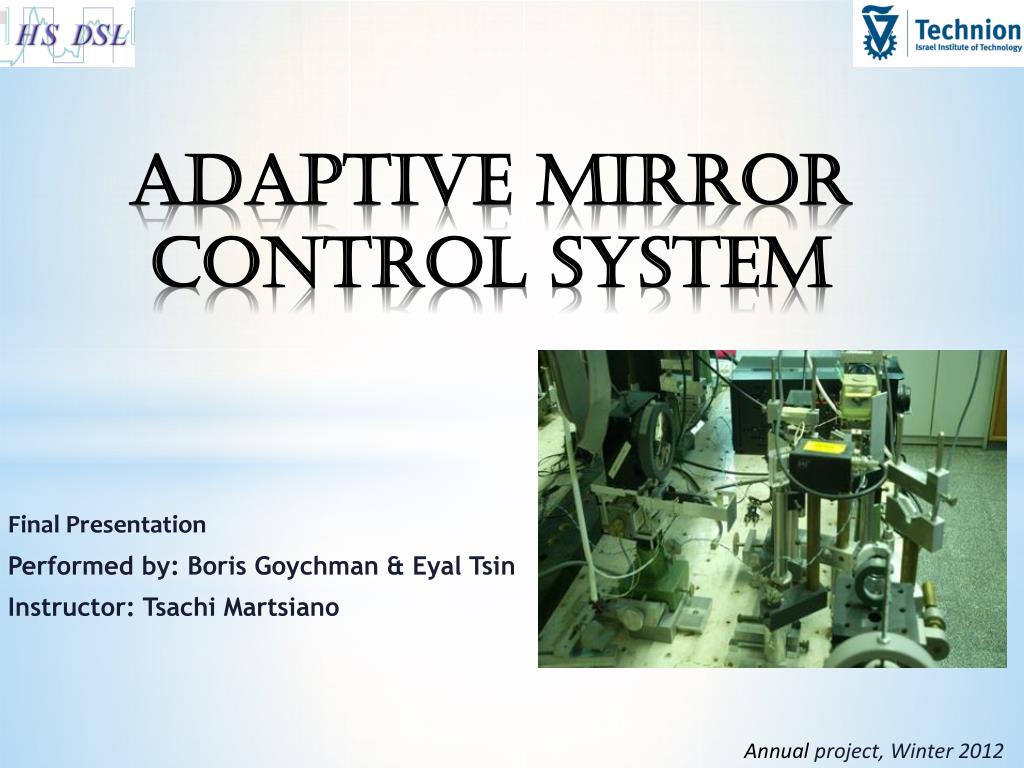
Adaptive Mirror Control System. Final Presentation Performed by: Boris Goychman & Eyal Tsin Instructor: Tsachi Martsiano. Annual project , Winter 2012. Joint project with physics faculty, deals with an adaptive mirror The mirror:
Adaptive Mirror Control System - slide 1
01 / 17Adaptive Mirror Control System
1 / 17

Télécharger la présentation

Adaptive Mirror Control System
Une image / un lien ci-dessous est fourni (tel quel) pour télécharger la présentation

Politique de téléchargement : le contenu du site vous est fourni TEL QUEL pour votre information et votre usage personnel ; il ne peut être vendu, concédé sous licence ni partagé sur d’autres sites sans l’accord de son auteur.Le contenu vous est fourni TEL QUEL, pour votre information et votre usage personnel uniquement. Téléchargez la présentation en cliquant sur ce lien. Lors du téléchargement, si vous ne parvenez pas à télécharger une présentation, l’éditeur a peut-être supprimé le fichier de son serveur.Pendant le téléchargement, si vous ne parvenez pas à obtenir une présentation, le fichier a peut-être été supprimé par l’éditeur.

F I N

Plus de contenu associé

Transcription de la présentation
  1. Adaptive Mirror Control System Final Presentation Performed by: Boris Goychman & Eyal Tsin Instructor: Tsachi Martsiano Annual project, Winter 2012

  2. Joint project with physics faculty, deals with an adaptive mirror • The mirror: • Changes Convexity in order to correct distortions of light originated in the atmosphere • Now used for eye retina distortion corrections Background

  3. Build a system that interfaces with a PC from one end and controls an adaptive mirror on the other. *Adaptive Mirror – contains 59 capacitors to control the shape of the mirror • Learn an approach for practical engineering. • Get familiar with FPGA, Logic Design and board design basics. Projects Goals

  4. Part B Part A BOARD DE2 - FGPA ALTERA CHIP D2A HV S&H HV S&H System Overview DLP - USB PC DLP CHIP GUI

  5. Specifications

  6. System Rates (timing analysis)

  7. Microprocessor • Philips provide software and drivers, easy to implement • Need to buy one + external RAM • Board design • FPGA design • Predesigned board • Difficult to test and design with VHDL • Choosing alternative USB control – ISP • Difficult interface • Higher rate (12Mbps) Development alternatives

  8. VHDL implementation • At least 4 FSM’s and some TBs • FPGA implementation selected • Due to availability • DLP_USB_245 • Simple FIFO – works! Devised solutions

  9. Control a 59 capacitor adaptive mirror • 256 voltage values for each capacitor • Same controller can be used to control any other system with the same requirements • 59 inputs or less • 256 values per input • The output of the D2A will pass through • a SAMPLE & HOLD (not in the scope of part A) • and then to the mirror (not in the scope of part A) System usage & possible expansions

  10. Data flow

  11. חבילת עדכון אחת של הקבלים במחשב 6bit capacitor 8bit voltage 00 59 ערכים HV_A 6bit capacitor 8bit voltage 00 USBtransfer 5 bit control MANAGER DLP’s FIFO FPGA’s FIFO LAST LAST D2A 8bit 6 00 8bit 8 bit control 1* 8bit 5 2 8bit 8bit 8bit 8bit 8bit Packets Split 8 bit control 8bit 8bit HV_B 5 bit control 8bit 6 00 8bit 1* 8bit 5 2 8bit 8bit 8bit FISRT FIRST * בוחר את אחד ה-HVים

  12. General Block Diagram Ext_SD_KEY1 Ext_RESET_KEY2 Ext_START_KEY0 D2A Controller MANAGER D2A DLP_ Controller DLP245- USB D_inout[7..0] HV257 Controller SWITCH- ADG202AKN D[7..0] full wrreq RELAY-AQY274 (SC)FIFO sclr S&H-HV257 rdreq S&H-HV257 Q[7…0] empty MUX-ADG784

  13. Designed FSM’s and coded VHDL for: • D2A Controller • DLP Controller • FIFO • HV Controller • Manager • Simulated and Emulated FSM’s for: • D2A Controller • DLP Controller • DLP Controller + FIFO • DLP Controller + FIFO + Manager • HV Controller What we have done in Part A

  14. Tested FSM’s with: • D2A+DVM • Emulation + Leds + 7 segment • Signal Tap What we have done in Part A

  15. Design and test the analog electric circuits : • D2A support circuit • DLP (USB) support circuit • HV support circuit • MUX, RELAY and SWITCH support circuits • 300V, +15V and -15V power supply • Integrate and test every-thing What we will do in part B

  16. Schedule

  17. Questions