Advanced Characterization Techniques of Dislocations and Surface Potentials in GaN Devices
120 likes | 234 Vues
This work highlights potential electronic characterization methods focused on dislocation behavior and surface potential variations in GaN-based devices, including HFETs. Key methodologies include AFM scanning probe measurements, UV light patterning, and scanning capacitance microscopy, which effectively assess charge storage and conductivity. The results indicate the significance of surface morphology and potential profiles, with a spatial resolution down to 1-2 micrometers. This research provides valuable insights into improving device performance and understanding fundamental charge dynamics in semiconductor materials.

Advanced Characterization Techniques of Dislocations and Surface Potentials in GaN Devices
E N D
Presentation Transcript
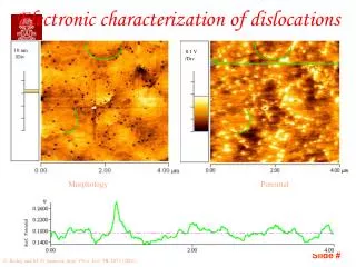
Goutam Koley Surf. Potential Electronic characterization of dislocations 0.1 V /Div 10 nm /Div Morphology Potential G. Koley and M. G. Spencer, Appl. Phys. Lett.78, 2873 (2001)
Goutam Koley UV light Surface potential patterning using mask 20 m circle quartz mask HFET Sample (35% Al in barrier, 44 nm AlGaN layer)
Goutam Koley Spatial resolution of charge storage UV exposure through a mask of 1, 2, 5, 10 and 20 m squares Spatial resolution on the order of ~1-2 m 3.5 m G. Koley et al. JAP (2004)
Goutam Koley AFM scanning probe Measurements in GaN based transistors Biasing Probes
Goutam Koley Drain Source Surface morphology and potential profiles in dc biased transistors Gate Vd = 2V, Vg = -1.5 V Morphology Surface Potential
Goutam Koley Measurement of transients AFM scanning probe Measurement setup schematic Probe tip Drain Source Gate Gate Drain A A Source 20 resistor +ve dc bias -ve dc bias or square pulse Biasing Probes G. Koley et al. IEEE Trans. Electron Dev. 50, 886 (2003) Goutam Koley
Goutam Koley Stressed at Vg = -12V, Vd = 20 V for 2 mins Maximum variation observed ~0.3 m from the gate edge Charges take a long time to reach equilibrium value Potential variation with distance and time 150 m HFET G. Koley et al. IEEE Trans. Electron Dev. 50, 886 (2003) Goutam Koley
Goutam Koley Surface conductivity measurements (a) Morphology, (b) conductivity, and (c) overlap of the surface morphology and conductivity images
Goutam Koley Scanned gate microscopy Scanned gate microscopy is useful to determine the variation of conductivity along a thin channel, and where direct measurement of conductivity is difficult (a) Experimental set up for SGM, (c) the SGM image of a single-walled CNT bundle for Vtip = 1 V; Black corresponds to very high resistance.
Goutam Koley Scanning capacitance microscopy Scanning capacitance technique actually measures the dC/dV signal which is inversely proportional to doping. The advantages of this technique include a large measurement range (1015 – 1020 cm-3), and resolution of <10 nm For capacitance measurement a low frequency ac voltage is applied to the sample. The ac voltage periodically changes the tip-sample capacitance. The sensor produces a high frequency signal to measure very small capacitance changes.
Goutam Koley Application of capacitance microscopy Cross-sectional measurement in a MOSFET under actual operation
Goutam Koley The dC/dV decreases around the dislocations indicating the reduction in the background carrier concentration Applications to GaN samples Capacitance image Morphology image C-V curve