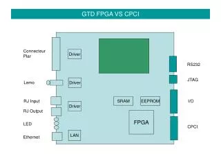
FPGA Master and Slave Communication Module for DAC and ADC Control
This document describes the architecture and functionality of a dual FPGA system designed for controlling Digital-to-Analog Converters (DAC) and Analog-to-Digital Converters (ADC). The Master FPGA interfaces with multiple Slave FPGAs to manage configuration, data transfer, and calibration of DAC outputs and ADC inputs. It highlights the communication protocols, signal routing, and pin configurations necessary for efficient operation within a complex data acquisition environment. Key features include signal multiplexing, calibration selection, and data enable/disable functions.

FPGA Master and Slave Communication Module for DAC and ADC Control
E N D
Presentation Transcript
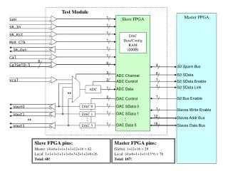
DAC 0 DAC 1 DAC 5 Test Module Master FPGA 1 Slave FPGA SaH 1 SR_In 1 SR_Rst DAC Data/Config RAM (300B) 1 MUX Clk 1 SR_Out 1 Cal 6 6 4 CalSel0-5 S0 Spare Bus 3 6 S0 SData ADC Channel 1 2 Vcal ADC Control S0 SData Enable 1 1 ADC S0 SData Link ADC Data 1 2 S0 Bus Enable DAC Control 1 Vout0 DAC SData 0 1 Slaves Write Enable 1 DAC SData 1 Vout1 12 Slaves Addr Bus 16 1 DAC Data 5 Vout5 Slaves Data Bus Slave FPGA pins: Master: (4)+6+1+1+1+1+12+16 = 42 Local: 1+1+1+1+1+1+6+3+2+1+2+6=26 Total: 68! Master FPGA pins: Global: 1+12+16 = 29 Local: (4)+6+1+1+1=13*6 = 78 Total: 107!