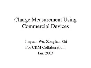
Charge Measurement Using Commercial Devices
Charge Measurement Using Commercial Devices. Jinyuan Wu, Zonghan Shi For CKM Collaboration. Jan. 2003. Introduction. FPGA. Q. Integrator. AD6644. PMT. HP1662C. The Circuit Board. AD6644. To Analyzer. Integrator (2) OPA660. Input Pulse. Integrator(1) AD8055. FPGA. EPC2LC20.

Charge Measurement Using Commercial Devices
E N D
Presentation Transcript
Charge Measurement Using Commercial Devices Jinyuan Wu, Zonghan Shi For CKM Collaboration. Jan. 2003
Introduction FPGA Q Integrator AD6644 PMT HP1662C
The Circuit Board AD6644 To Analyzer Integrator (2) OPA660 Input Pulse Integrator(1) AD8055 FPGA EPC2LC20 Optical receiver SLC-25-4 Transceiver TLK1501
Outline • AD6644. • Integrator circuit (1). • ADC output. • Optical Transmission. • Integrator circuit (2).
Commercial ADC: AD6644 • The AD6644 is a high speed, high-performance, monolithic 14-bit analog-to-digital converter. • The guaranteed sample rate is 65 MSPS. • The sample rate in our tests is 35 MHz or • the sample time is 28.5ns. • Current FPGA technology is used in our • tests.
Integrator for ADC [1] 100pf 36.5k _ Input Pulse OUTPUT 51 AD8055 + GND +2.5V • It is a traditional integrator. • T=RC=36.5k x 100pf=3.65us=128 x 28.5ns • The output will send to AD6644 as a input signal.
InputPulse Output
Input Pulse Output
Digital Process of AD6644 Output ADC ADCQ = Charge D • Using FPGA hardware to find charge. D DIFF ABS SUB AND Higher Bits OR Simple Zero Suppression Algorithm
Data from HP 1662C Logic Analyzer ADCQ DIFF =Charge
D The Stability of AD6644 D(DATAFROM AD6644) S SUB ABS D R(RESULT) EN 256 • DC input is sent to AD6644. • Above circuit is used to produce the mean of absolute difference.
Data From HP 1662C Logic Analyzer Result ADCQ
Optical Transmission • The ADC test board has same interface as the QIE test board. • Data have been successfully transmitted to Lab 6 station. • A simpler test station is being built at WH14W.
100pf 5V Integrator for ADC [2] 36.5k 8 OUTPUT 150 3 Input Pulse OPA660 51 2 Operational Amplifier & Buffer GND 17 GND 150 5 6 +1 Similar as Ken Nelson’s design except the omission of the reset circuits. 51 GND
Input Pulse Output
Input Pulse Output
Thanks END
Input Pulse Output Integrator (1)
Input pulse Output Integrator (2)