Understanding Charge-Coupled Devices and Semiconductor Memories: Mechanisms and Applications
70 likes | 191 Vues
This article explores the principles and operations of Charge-Coupled Devices (CCDs) and semiconductor memories, specifically Dynamic Random Access Memories (DRAMs) and their utilization of MOS capacitors. It discusses the generation of charge carriers in CCDs via optical means, the importance of inversion layers, and the necessity of refreshing DRAMs. Additionally, the text examines the working of MOS capacitors in different voltage conditions and elaborates on the characteristics of both volatile and non-volatile memories. Key applications in imaging and signal processing are highlighted.

Understanding Charge-Coupled Devices and Semiconductor Memories: Mechanisms and Applications
E N D
Presentation Transcript
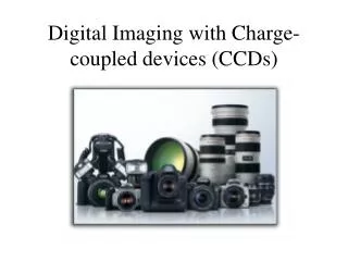
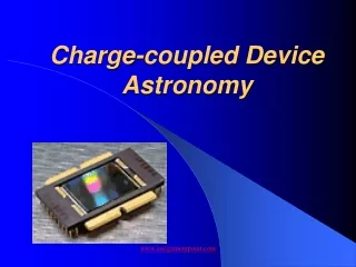
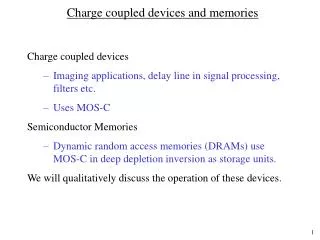
Charge coupled devices and memories • Charge coupled devices • Imaging applications, delay line in signal processing, filters etc. • Uses MOS-C • Semiconductor Memories • Dynamic random access memories (DRAMs) use MOS-C in deep depletion inversion as storage units. • We will qualitatively discuss the operation of these devices.
M O S M O S p-Si p-Si VG < 0 VG > 0 Accumulation of holes W QM Depletion of holes MOS-capacitor - review Consider ideal case, with p-type Si VG < 0 accumulation VG > 0; depletion, but less than VT
M O S M O S p-Si p-Si VG>>0 VG>>0 WT QM Depletion of holes Inversion electrons MOS-capacitor - review VG >> 0; VG > VT Steady state inversion condition Depletion layer = WT VG >> 0; VG > VT applied instantaneously. W is larger than WT. W QM After a few ms, you get steady-state condition, and W reduces to WT. Inversion layer forms Depletion of holes
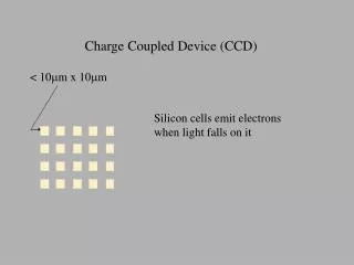
Time required to form inversion layer • It take a few milli-seconds to form the inversion layer since they are caused by minority carriers. Depends on e-h generation rate • can generate faster by optical means • can generate by injection of electrons from n+source and drain if present in close proximity • can increase the temperature to increase e-h generation rate or by introducing deep levels. • In CCDs, e-h pairs are generated by optical means, and generation by thermal means must be kept to a minimum (Why?)
CCD operation region oxide electrons depletion VT Concept of CCD imager • Generation in depletion layer light intensity • i.e., inversion layer charge light intensity • Read out of charge pulse amplitude by operating as shift registers • Need to read out sequentially fast enough such that the thermal generation of carriers can be neglected. • 3- clock provides directionality. CG Al VG
Memories • Logic devices that store and manipulate information. • Random access and sequential access. • Semiconductor Memories • non-volatile memory • ROM, PROM, EPROM, E2PROM • Volatile memories • DRAM - need to refresh every few ms. • SRAM - no need to refresh • One transistor DRAM cell • high density, but requires complex read/write/refresh circuits.
One transistor DRAM cell Column bit or data line (BL) Row Word line (WL) CS VP A stored one will be deep depletion condition. A stored zero will be the inversion condition. Note that a stored one will revert to zero if not refreshed. Need refreshing every few milliseconds.