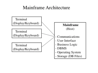
Host/Memory/User Interface
Host/Memory/User Interface. Interfacing with the host computer, external memory, and user. ESU: Extended Parallel Port, Smart Media Card, and User Interfaces. ESU Memory Mapped Registers. Timing

Host/Memory/User Interface
E N D
Presentation Transcript
Host/Memory/User Interface Interfacing with the host computer, external memory, and user
ESU: Extended Parallel Port, Smart Media Card, and User Interfaces
Timing Programmed by software (probably the boot routine) this register sets parameters for all of the critical timing between the DSP and the Smart Media Card. Each of the timing blocks is a 3 bit number which will be used as a index to a counter. Therefore the smallest number we can count for is our cycle time (10ns). This 3 bit limitation means that the longest we can hold a signal for is 70ns. The longest requirement for our SMC is 50ns. Data The data register is a bi-directional register which can be written and read by the SMC, the EPP, and the Data Bus. The first byte of the data register is designated for the SMC (which has an 8 bit I/O bus), and the second for the EPP. Command/Status The command/status register takes care of all other functions. It is polled and written regularly by both software and the host. Additionally the last byte of this register can be written by eight external buttons (user controls). The first four bits specify the SMC operation that software wants to perform and are read by the SMC_SIG_GEN unit to carry out that operation. Bit four is the SMC R/nB, which indicates if a SMC operation is running. Bit 5 is the SMC data read bit, which goes hi when there is valid data from the SMC in the data register. Bit six is the EPP status bit, it indicates if there is data in the data register. This bit can be written by both the host and the software, and therefore must be polled before the data register is written by either. ESU: Memory Mapped Register Descriptions
SMC Commands * Data must be valid in the Data register before the command is programmed in the cmd/status register
Example operations • READ: Commands: CMD Addr1 Addr2 Addr3 Read1 Read … Reset Data: <00h> <a1> <a2> <a3> <Din> <Din> …<XX> • Write: Commands: CMD Addr1 Addr2 Addr3 Write Write … Write CMD CMD Read1 Data: <80h> <a1> <a2> <a3> <Dout> <Dout> … <Dout> <10h> <70h> <stat> • Erase: Commands: CMD Addr1 Addr2 Wait CMD CMD Read1 Data: <00h> <a1> <a2> <XX> <D0h> <70h> <stat>