Download
1 / 1
10 likes | 203 Vues
U. H. BTO. BTO. LSMO. LAO. LSMO. (a). (b). (a). (d). (c). (b). NIRT: Composition Graded, Epitaxial Oxide Nanostructures: Fabrication and Properties NSF NIRT Grant # 0709293 Efstathios Meletis 1 , Jiechao Jiang 1 , Chonglin Chen 2 , Amar S. Bhalla 2 , and Gemunu Gunaratne 3

E N D
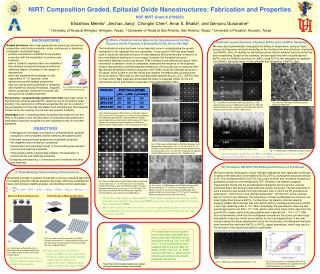
U H BTO BTO LSMO LAO LSMO (a) (b) (a) (d) (c) (b) NIRT: Composition Graded, Epitaxial Oxide Nanostructures: Fabrication and Properties NSF NIRT Grant # 0709293Efstathios Meletis1, Jiechao Jiang1, Chonglin Chen2, Amar S. Bhalla2, and Gemunu Gunaratne3 1 University of Texas at Arlington, Arlington, Texas; 2 University of Texas at San Antonio, San Antonio, Texas; 3University of Houston, Houston, Texas BACKGROUND (II) Effects of Substrate Surface Miscut on the Two-dimensional Interface Structures and the Properties of Epitaxial (Ba,Sr)TiO3 film on (001) MgO (III) Double Layered Structures of Epitaxial BaTiO3 and (La,Sr)MnO3 Nanopillars Graded structures with a high perpendicular anisotropy arising from composition and structure variation, either continuously or discretely (composite, modulated layers): We have also systematically investigated the effects of temperature, pressure, laser energy and frequency and post-annealing on the formation the microstructure of epitaxial (La,Sr)MnO3 films. A roadmap for fabricating various distinct epitaxial nanostructures has been established. Based on the roadmap, we fabricated films with a double-layered BaTiO3 and (La,Sr)MnO3 structure on LaAlO3 using PLD by first fabricating an epitaxial (La,Sr)MnO3 nanopillar layer on the substrate and followed by a BaTiO3layer. The interfacial structure has been a very important issue in understanding the growth mechanism of the epitaxial films and nanopillars. Cross-section TEM has been widely used to study the interfacial structure of heteroepitaxial films and has been turned out to be a very effective technique for such cases. However, the interfacial structure information obtained using cross-section TEM is limited in one-dimensional space. More information is needed in order to completely understand the influence of the substrate surface characteristics and film/substrate interface on the microstructure of epitaxial films. We recently developed a method using plan-view TEM to study the interface structure in 2D space, which is able to provide critical and valuable information that is lacking from the cross-section TEM analysis. We have fabricated epitaxial Ba0.6Sr0.4TiO3 (BSTO) films on miscut (001) MgO substrate and studied the effect of substrate miscut on the 2-D interfacial structure and dielectric properties of the epitaxial BSTO films. • produce coexistence of different cross coupled properties with the expectation to produce new materials. • have a “product” property that is not available in the individual component phases providing an additional degree of freedom in the design of nanodevices. • yield new fundamental knowledge on self-organization of 1-D, epitaxial, oxide nanostructures with graded composition. • open up various new possibilities of designing new multiferroic (having ferroelastic, magnetic, electric properties) nanoscale structures with unusual cross coupled properties. Fig. 1 Project flow chart for strategy of fabricating graded structures Ferroelectric, compositionally gradient thin films have been shown to tremendously enhance piezoelectric response due to the build-in strain gradient. The coexistence of different properties that can be coupled in nanocomposite thin films has stimulated much scientific and technological interest since the coupling can provide new property tenability. Challenges exist in extending these compositional variations from thin films to nanopillars since the fabrication of compositionally graded and modulated composite nanopillars by self-organization has not yet been attempted. Fig. 8 Plan-view TEM image) of the double layered BaTiO3/(La,Sr)MnO3 film. Fig. 7. (a) XTEM of a double-layered BaTiO3/(La,Sr)MnO3 on (001) LaAlO3 substrate. (b) and (c) SAED patterns taken from the LSMO/LAO interface and the BTO layer, respectively. (d) Dark-field image obtained using the common (011) spot of BTO, LSMO and LAO. Table 1 Dielectric properties of BST thin films on (001) MgO measured at 300 K and 2 GHz. The films grown on 1.2º and 5.3º miscut substrates show significantly higher dielectric constant and dielectric tunability, which are about 30% more than those for the film grown on 3.5º miscut substrate. The variations in property are attributed to misfit strain difference and the resulting variations in the microstructure of the films. OBJECTIVES • Investigate the principles of formation of self-assembled, epitaxial nanopillars of ferromagnetic and ferroelectric perovskite-oxides • Fabricate compositionally graded and modulated composite ferromagnetic and ferroelectric nanopillars • Characterize and mechanism study of the morphological evolution, structure and physical properties • Theoretically identify relationships between characteristics of nanostructures and materials properties • Designing and exploring 1-D nanostructures of interest and other new materials Fig. 4 XTEM image and SAED patterns of BST/MgO deposited on the substrate with a miscut angle of 1.2º (a, d); 3.5º (b, e) and 5.3º (c, f). The lattice mismatch between the film and substrate obtained from (a), (b) and (c) is about -5.4%, -5.7% and -5.5%, respectively.No significant structural difference can be observed in the 1-D interface space. Fig. 9 XTEM image of BTO/LSMO double layer on LAO. Fig. 10 HRTEM images of BTO/LSMO nanopillars’ Interface Epitaxial quality double layered BTO and LSMO nanopillars can be successfully fabricated using PLD up to a thickness of ~200 nm. (IV) Ferroelectric BaTiO3/SrTiO3 Multilayered Structures on Si Substrate (I) Theory/Modeling: Self-assembling of Nanostructures We have recently developed a unique interface engineered nano fabrication technique to achieve the fabrication of ferroelectric BaTiO3/SrTiO3 multilayered structures directly on Si. The multilayered BaTiO3/SrTiO3 has a ratio of 60/40 and should be formed as a paraelectric phase at room temperature (RT). However, the dielectric property measurement shows that the as-fabricated multilayered structures have unusual hysteresis loops with strong locked polarized domain structures. The ferroelectricity of such a structure was evident from the hysteresis loop, in which the RT spontaneous polarization, ~200 mC/cm2, and remnant polarization, 100 mC/cm2, with a coercive field of 10 kV/cm are obtained. The polarization of these multilayered structures is one order higher than the pure BaTiO3. Furthermore, the dielectric and ferroelectric property studies demonstrated that such BaTiO3/SrTiO3 multilayered structures exhibit a very high resistivity value of 1011 Wcm. Especially, the piezoelectric response was surprisingly found to be 540 x 10-12 C/N, which is about five times of the value from the pure BaTiO3 single crystal and polycrystalline bulk materials [90 – 100 x 10-12 C/N]. Such achievements show that the multilayered ferroelectric structures can have large piezoelectric response, which are promising for the future applications of the new concept advanced device development since the introducing of multilayered interfaces have brooked the traditional BaTiO3 or SrTiO3 crystal symmetries, which may result in the recovery of the vacant piezoelectric coefficients. We studied a model of quantum dot growth to test our proposed algorithm for creating perfectly ordered quantum dot arrays. We have conducted its linear and nonlinear stability analysis, and identified control parameters. Fig. 5 Plan-view SAED pattern of the BST/MgO interface on MgO with a miscut angle of (a) 1.2º; (b) 3.5º (b) and (c) 5.3º ; (d) schematic illustrate of the diffraction spots of thediffraction patterns. The lattice mismatched obtained from (a), (b) and (c) is -5.6, -6.0% and -5.7%, larger than those obtained from the XTEM analysis. Significant structural difference can be observed in the SAED patterns. Fig. 6 (a), (b) and (c) XTEM images of the BST/MgO interface on MgO with a miscut angle of 1.2º, 3.5º and 5.3º, respectively. No distinct differences was found.(d), (e) and (f) plan-view TEM images of the interface on MgO with a miscut angle of 1.2º, 3.5º and 5.3º, respectively. Different commensurate domains size were observed. Defective Self-assembly Arrays Perfect Arrays in Masked Deposition • 2D interface study allows to obtain actual or “local” lattice mismatchat the interface, which generally larger than that obtained using XTEM and provide critical and valuable information that is lacking from XTEM • Miscut of the substrates alters the surface structural configuration, produces extra local strain and modification of local structure of the interface and dramatically changes the dielectric properties of the films. The specifications and long term vision have been discussed with the project team members during the kickoff meeting (Oct. 1st, 2007, UTA). These specifications were updated during the 2nd (May 26, 2008, UTSA), 3rd (Oct. 16, 2008, UH) and 4th (Nov. 6, 2009) project meeting according to the project feedback mechanism. Fig. 3 (a) A mask to control the deposition, (b) Ordered monolayer self-assembly, (c) Ordered quantum dot arrays and (d) ordered array of inverted quantum dots that can be filled with –say- a magnetic material. Fig. 2 (a) Monolayer self-assembly and (b) a typical large-scale self-assembled quantum dot array contains multiple domains, domain walls and other defects. • Placing a mask above the substrate: • atoms can diffuse to sites under mask • breaks the region into small segments smaller than the domain size • width of the mask < diffusion length; atoms can drift on the entire substrate Devices made from such arrays will have inhomogeneous optical and electrical properties. Fig.12 Dielectric property of a multilayered BaTiO3/SrTiO3 showing an unusual hysteresis loop suggesting the locked domain polarizations in the nanostructures. Fig.11 XTEM image of multilayered BaTiO3/SrTiO3 on Si. Project flow chart for interaction between team members and overall contribution to Design of new materials.