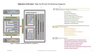
Bus Architecture
320 likes | 492 Vues
This text explores the architecture of a 16-bit bus system used in CSC321, detailing components like Memory Units, ALU, and Control Unit. It examines instruction formats, including direct and indirect addressing, and explains register operations such as CLA, CLE, INC, and branch instructions. The flow of instruction execution is presented, highlighting timing phases T0 to T5, with examples of how to fetch, decode, and execute instructions. The design principles of control units and the significance of the sequence counter in managing instruction execution are also discussed.

Bus Architecture
E N D
Presentation Transcript
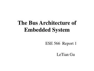
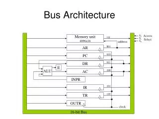
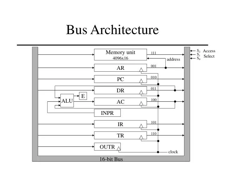
Bus Architecture S2 Access Select Memory unit 4096x16 111 S1 S0 address 001 AR 010 PC 011 16-bit Bus DR E ALU 100 AC INPR 101 IR 110 TR OUTR clock CSC321
Instruction Format 15 14 12 11 0 I opcode address I = 0 means direct memory address I = 1 means indirect memory address CSC321
The Control Unit Instruction Register (IR) 15 14 - 12 11 - 0 Other Inputs 3x8 Decoder 12 Control Unit D7 – D0 n I T15 – T0 4x16 Decoder Increment Sequence Counter Clear Master Clock CSC321
Decoding the Instruction • We seen how to fetch and decode instructions in RTL notation • We now need to look at how to execute each instruction T0 T1 T2 = 1, register or I/O = 0, memory reference = 1, I/O = 0, register = 1, indirect = 0, direct T3 T3 T3 T3 CSC321
Register Instructions • These are all pretty simple • CLA D7I’T3B11: AC ← 0 • CLE D7I’T3B10: E ← 0 • CMA D7I’T3B9: AC ← AC’ • CME D7I’T3B8: E ← E’ • CIR D7I’T3B7: AC ← shr(AC), AC(15) ← E, E ← AC(0) • CIL D7I’T3B6: AC ← shl(AC), AC(0) ← E, E ← AC(15) CSC321
Register Instructions • INC D7I’T3B5: AC ← AC + 1 • SPA D7I’T3B4: if (AC(15) = 0) then (PC ← PC + 1) • SNA D7I’T3B3: if (AC(15) = 1) then (PC ← PC + 1) • SZA D7I’T3B2: if (AC = 0) then (PC ← PC + 1) • SZE D7I’T3B1: if (E = 0) then (PC ← PC + 1) • HLT D7I’T3B0: S ← 0 • S is a flip-flop that starts/stops the master clock CSC321
Register Instructions • Perhaps the most interesting thing about these instructions is the condition on which each is selected • D7I’T3Bi • The D7I’terms specify the type of operation (register) • Execution starts at time T3 since no additional operands need to be fetched from memory • The Bi term is the interesting one CSC321
Register Instructions • Note how the opcodes were assigned hex (binary) bit patterns • Notice any patterns? • Very common practice in both hardware design and programming CSC321
Memory Instructions • The condition on which each is selected comes from the decoding of the operand and starts at time T4 • DiT4 • The Di term specifies the particular operation • Execution starts at time T4 assuring the operand has been fetched from the effective address CSC321
Memory Instructions • These are a bit more complex • AND operation • D0: AC ← AC ^ M[AR] • This is fine except for the fact that the operation must take place in the ALU and M[AR] cannot be routed there directly • Therefore, we must rework this functional RTL statement to reflect the actual hardware architecture CSC321
Logical AND • We must first get M[AR] into the DR register • Then we can perform the AND operation D0T4: DR ← M[AR] D0T5: AC ← AC ^ DR, SC ← 0 • Requires two timing phases, T4 and T5 CSC321
Arithmetic ADD • Similar in nature to the AND operation D1T4: DR ← M[AR] D1T5: AC ← AC + DR, E ← Cout, SC ← 0 • The result remains in the AC register • If we want to place it in memory we must perform a store (STA) instruction CSC321
Load Accumulator • Similar in nature to the AND operation D2T4: DR ← M[AR] D2T5: AC ← DR, SC ← 0 • Recall that the AC is only accessible through the ALU • This is why one of the ALU functions was a transfer (without any arithmetic operation) CSC321
Store Accumulator • Similar in nature to the AND operation D3T4: M[AR] ← AC, SC ← 0 CSC321
Branch Unconditionally • A branch is merely a modification of the program counter (PC) register D4T4: PC ← AR, SC ← 0 CSC321
Branch and Save Return Address • BSA is the assembly language version of a subroutine call • It must store the address of the next instruction (which is in the PC since we incremented it after the fetch cycle) somewhere • It uses the effective address of the operand for this purpose • It then performs a branch to the subroutine address CSC321
Branch and Save Return Address D5T4: M[AR] ← PC, AR ← AR + 1 D5T5: PC ← AR, SC ← 0 • This means that the subroutine actually starts one memory location after that specified in the operand • Consider an example… CSC321
After time T5 (when the instruction is complete) the PC is here After time T3 the PC is here 0x20 0x20 0 BSA 0x50 0 BSA 0x50 0x21 0x21 0x50 0x50 0x21 0x51 0x51 SUBROUTINE CODE SUBROUTINE CODE 1 BUN 0x50 1 BUN 0x50 BSA instruction inserts this at time T4 Programmer inserts this command Branch and Save Return Address CSC321
Increment and Skip if Zero • This is used for creating for loops • Typically, you will store a negative loop count prior to using an ISZ command • It is also used in coordination with a BUN instruction D6T4: DR ← M[AR] D6T5: DR ← DR + 1 D6T6: M[AR] ← DR, if (DR = 0) then (PC ← PC + 1), SC ← 0 CSC321
Calculate loop count into AC Store loop count 0x20 0 STA 0xAA 0x21 Start of loop End of loop 0x50 0x51 0 ISZ 0xAA 0 BUN 0x21 -810 0xAA 0xFFFC Increment and Skip if Zero CSC321
Input/Output Instructions • Three new flip-flops are introduced into the architecture to support input/output commands • FGI – 1 when information from the input device is available, 0 otherwise • FGO – 1 when the output device is ready to receive information, 0 otherwise • IEN – interrupt enable CSC321
Input/Output Instructions • INP D7IT3B11: AC(0-7) ← INPR, FGI ← 0, SC ← 0 • OUT D7IT3B10: OUTR ← AC(0-7), FGO ← 0, SC ← 0 • SKI (used in a manner similar to the ISZ) D7IT3B9: if (FGI = 1) then PC ← PC + 1, SC ← 0 • SKO (used in a manner similar to the ISZ) D7IT3B8: if (FGO = 1) then PC ← PC + 1, SC ← 0 CSC321
Input/Output Instructions • A problem arises when using the SKI and SKO instructions • Their purpose is to set up loop structures (similar to what we saw with the ISZ instruction) waiting for an input/output device to become available • This could cause large amounts of valuable time to be wasted CSC321
Interrupts • To alleviate this problem we introduce interrupts into the system • Two instructions enable and disable interrupts • Sometimes we don’t want to be interrupted such as when we’re doing something important or we’re already servicing and interrupt • ION (enable interrupts) D7IT3B7: IEN ← 1, SC ← 0 • IOF (disable interrupts) D7IT3B7: IEN ← 1, SC ← 0 • We also introduce another flip-flop, R, which tells the system when there is an interrupt to be handled CSC321
Interrupt Cycle • Interrupts are subroutine calls with a couple of differences • They come at arbitrary times during program execution • The start address of the interrupt service routine (subroutine) is a predetermined, fixed location in memory CSC321
Set up the interrupt service routine I/O device is ready so signal an interrupt Once set-up, the system carries on as usual Interrupt Cycle The interrupt service routine ends with a BUN to indirect address 0 = 0 = 1 = 0 = 1 = 1 = 0 = 1 = 0 CSC321
Interrupt cycle sets return address here and PC here PC is here when the interrupt occurred 0x00 0x00 0x11 0x01 0x01 0 BUN 0x51 0 BUN 0x51 0x10 0x10 0x11 0x11 0x51 0x51 INTERRUPT SERVICE ROUTINE INTERRUPT SERVICE ROUTINE 1 BUN 0x00 1 BUN 0x00 Interrupt Cycle CSC321
Interrupt Cycle Implementation • To implement the interrupt cycle we introduce the R flip-flop\ • To utilize it we modify our fetch/decode RTL as follows CSC321
Modified Fetch/Decode • It was this… • We modify it to this… T0: AR ← PC T1: IR ← M[AR], PC ← PC + 1 T2: D0, … D7 ← Decode IR(12-14), AR ← IR(0-11), I ← IR(15) R’T0: AR ← PC R’T1: IR ← M[AR], PC ← PC + 1 R’T2: D0, … D7 ← Decode IR(12-14), AR ← IR(0-11), I ← IR(15) CSC321
Modified Fetch/Decode • We must also add the interrupt cycle handler RTL… RT0: AR ← 0, TR ← PC RT1: M[AR] ← TR PC ← 0 RT2: PC ← PC + 1, IEN ← 0, R ← 0, SC ← 0 CSC321
Remainder of Chapter 5 • The remainder of the chapter discusses how to convert the Control Unit RTL into logic gates • This is really nothing more than defining AND/OR/NOT/XOR gates to handle the conditions on the RTL statements • Thus, I’m not going to spend any time on it and won’t hold you accountable for it but… • You should read it over once to get a feel for how all this stuff ties together CSC321
Homework • Pages 167, 168 • Problems 5-1, 5-2, 5-3, 5-4, 5-5, 5-6, 5-9, 5-10, 5-11, 5-12 • Absolutely due on Tuesday April 13, 2004 • We will be going over the answers in class that day in preparation for exam 2 on Thursday April 15, 2004 CSC321