Download
1 / 17
170 likes | 344 Vues
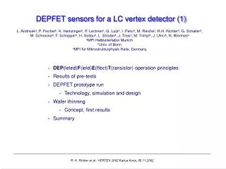
Status of DEPFET sensors. JRA1 Design Review Meeting Geneva, 28.01.2007 Stefan Rummel on behalf of the DEPFET collaboration. Overview. DEPFET principle Status of the PXD5 production Goals of the new production Wafer design, Chip overview R&D towards an ILC module concept

E N D
Status of DEPFET sensors JRA1 Design Review Meeting Geneva, 28.01.2007 Stefan Rummel on behalf of the DEPFET collaboration
Overview • DEPFET principle • Status of the PXD5 production • Goals of the new production • Wafer design, Chip overview • R&D towards an ILC module concept • System aspects - new Hybridboard Stefan Rummel; MPI for Physics
DEPFET principle • Combination of detector grade silicon with first p-FET amplification stage in each pixel • Potential minimum for electrons is created under the channel by sideward depletion and an additional n-doping • Electrons in the “internal gate” modulate the transistor current • Signal charge is removed via a clear contact • Large sensitive volume due to the fully depleted bulk • Low noise caused by a small input capacitance and internal amplification • Transistor can be switched off by external gate – charge collection is then still active! Stefan Rummel; MPI for Physics
Production status - PXD5 • All implantations done • Polysilicon layers are deposited and structured • To be done: • Contact holes • Metal layer 1 and 2 • Backside (double sided process) • New devices available around June 07! Stefan Rummel; MPI for Physics
Goals of the PXD5 production • Technological improvements • Larger matrices • Long matrices (full ILC drain length) • Wide matrices (full Load for Switcher Gate / Clear chips) • Performance improvements: • Reduce clear voltages • Charge collection • Small pixels (20µm x 20µm) • Increase internalamplification (gq) • Bump bonding test structures Stefan Rummel; MPI for Physics
PXD5 PXD4 New feature – smaller gates • PXD4: matrices with 6µm gate length • PXD5: matrices with gate length down to 4µm • Aim for significant improvement in gain! • Less sensitive to external noise! Stefan Rummel; MPI for Physics
standard arrays compatible to existing hybrids wide arrays (512 x 512, full ILC) long arrays (256 x 1024, ½ ILC) various new standard arrays (64 x 256 pixels, down to 20x20µm2) Rainer Richter, MPI HLL PXD5 Wafer Stefan Rummel; MPI for Physics
Standard detector • 128 (x) x 64 (y) double pixels = 64 x 256 pixels • Various pixel sizes 32x24µm², 24x24µm², 20x20µm² chip size 7x10mm² • 2 x Switcher3, 1 x CURO • 50 devices per wafer • Provided in many design variations Stefan Rummel; MPI for Physics
Standard detector compatible to old hybrids • 64 (x) x 64 (y) double pixels = 64 x 128 pixels • Pixel size 32x24µm², chip size 7*7mm • 2 x Switcher2, 1 x CURO • 24 devices per wafer • Devices already incorporate new design features! Working systems with this devices will be available soon after the production is completed! Stefan Rummel; MPI for Physics
Wide detectors • 512 (x) x 256 (y) double pixels = 512 x 512 pixels (full ILC width). Pixel size 32 x 24 µm² • 2 x 2 x Switcher 3, 8 x CURO • 4 devices per wafer • Study full load on Switcher signals Stefan Rummel; MPI for Physics
Long detectors • 128 (x) x 1024 (y) double pixels = 128 x 2048 pixels (full ILC RO length). Pixel 24 x 24 µm² • 2 x 8 x Switcher 3, 2 x CURO • 2 devices per wafer • Study full load on drain signals to CURO Stefan Rummel; MPI for Physics
R&D towards an ILC module concept • Thinning technology shows significant progress • Full scale mechanical samples • Thinned (50µm) diodes show excellent leakage currents • Thinned DEPFET devices within the PXD6 production are possible! Stefan Rummel; MPI for Physics
Next generation steering chips • CURO successor • Better noise performance • ADC for every channel • In work • Switcher3 • 128 channels • Radiationhard design • 10V voltage swing • Already available! Stefan Rummel; MPI for Physics
New Hybrid boards • Larger devices need more steering- and readout chips • Require changes on: • Hybrid level • System level • Redesign of the Hybrid will start in February Hybrid board V2.0 Stefan Rummel; MPI for Physics
Summary • New production is approximately ready in June • Working systems with PXD5 devices will be available soon after production is finished • DEPFET is on a good way towards measurements with the Demonstrator Stefan Rummel; MPI for Physics
Backup…. Stefan Rummel; MPI for Physics
The PXD5 Wafer • 2 long arrays (256x1024 – half ILC length) • 24x24 µm² cells, chip size 8.5x55mm² • 4 wide arrays (1024x256 – full ILC width) • 32x24 µm² cells, chip size 21x20mm² • 50 128x128 test array for new hybrids • 32x24µm², 24x24µm², 20x20µm² • chip size 7x10mm² • 1 128x128 bump bond test array • 24x24 µm² cells, chip size 8.5x10mm² • 24 128x64 test arrays for old hybrids • PXD4-cells, 32x24µm², 24x24µm² • 45 16x6 mini matrices • 32x24µm², 24x24µm² • chip size 3.5x4mm² • 7 different chips with double cells • geometry var. of depmos and clear reg. • chip size 7x4mm² • 2 mixed chips (double cells and 1 minimatrix) • chip size 5x5mm² • 3 transistor chips, different p- and nMOS • chip size 7x4mm² • 10 technology chips test structures • 23 G.L. chips • 2 XEUS chips for simul. clear Stefan Rummel; MPI for Physics