Silicon sensors status
130 likes | 264 Vues
This document outlines critical design considerations for silicon sensors, particularly regarding pad array design, fabrication techniques for bias resistors and coupling capacitors. It contrasts polysilicon and punch-through resistors, emphasizing their production complexities and performance checking. Additionally, the pre-prototyping and electric characterization of diodes and bias resistors are examined, including I-V and C-V testing methodologies. The importance of long-term stability tests and the necessary equipment for accurate testing are also discussed to ensure sensor performance and reliability.

Silicon sensors status
E N D
Presentation Transcript
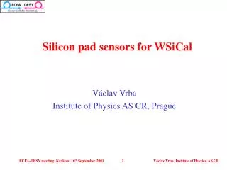
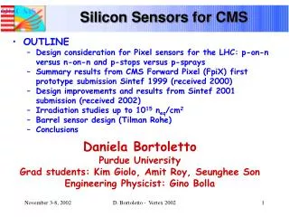
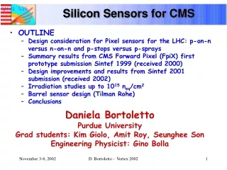
Silicon sensors status Václav Vrba Institute of Physics, AS CR, Prague Václav Vrba, Institute of Physics, AS CR
Pad array design consideration Along with the diodes, the technique used for fabrication of bias resistors and coupling capacitors represents an important issue: a) polysilicon resistors – production of the tile needs about 7-8 masks; can be the source of additional yield reduction. b) punch through resistors – production of the tile needs about 5 masks; easy to produce – needs to check whether required parameters can be achieved. c) ion implantation resistors – not considered here. Václav Vrba, Institute of Physics, AS CR
Design consideration: Polysilicon resistors Bias lines Top view Direct contact on diode – e.g. for testing Bias resistor Coupling capacitor Vertical cross section Václav Vrba, Institute of Physics, AS CR
Design consideration: Polysilicon resistors Václav Vrba, Institute of Physics, AS CR
Design consideration: Punch through resistors Bias lines Top view Direct contact on diode – e.g. for testing Bias resistor Coupling capacitor Vertical cross section Václav Vrba, Institute of Physics, AS CR
Design consideration: a partial summary a) polysilicon resistors: • should not be a problem to have resistors 10 M; • capacitors 1-10 nF. b) punch through resistors: • resistors to be tested; if acceptable then it is a simple solution; • capacitors as a). Compatibility of process for variants a)andb) on one wafer? Option a) as a baseline for main sensor tile? Václav Vrba, Institute of Physics, AS CR
Pre-prototyping Václav Vrba, Institute of Physics, AS CR
Tests outlines A) Diode tests a) I-V curves: • Vbreak-down Vop • Ileak @ Vop < cca 30 nA/cm2 b) C-V curves: • determination of Vfull-depletion; Vop = Vfull-depletion + 50 V. c) Long term stability tests: • Ileak @ Vop . Tile should be rejected if: • Vbreak-down< Vop • Ileak > I crit (to be defined). Václav Vrba, Institute of Physics, AS CR
Electric characterization Václav Vrba, Institute of Physics, AS CR
Tests outlines B) Bias resistors a) shorts b) breaks c) outside specifications C) Capacitance couplings a) shorts b) breaks c) outside specifications Václav Vrba, Institute of Physics, AS CR
Tests outlines Basic equipment: • micromanipulators with contact needles; • I-V: Keithley 487 A; • C-V: LCR meter HP Václav Vrba, Institute of Physics, AS CR
Probestation Václav Vrba, Institute of Physics, AS CR