Download
1 / 24
270 likes | 641 Vues
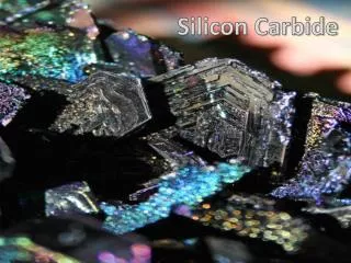
Silicon carbide thin films for EUV application deposited by means of Pulsed Laser Deposition (PLD). Gianni Monaco LUXOR-IFN Laboratory COST meeting Krakow , May 2010 COST-STSM-MP0601-05393 Report gmonaco@dei.unipd.it. Outline. SiC Carbides in the EUV; PLD systems ;

E N D
Silicon carbide thin films for EUV application deposited by means of Pulsed Laser Deposition (PLD) Gianni Monaco LUXOR-IFN Laboratory COST meeting Krakow, May 2010 COST-STSM-MP0601-05393 Report gmonaco@dei.unipd.it
Outline • SiCCarbides in the EUV; • PLD systems; • SiCthinfilmsdeposited at IOP-WAT WarsawwithExcimer laser; • Analysisof the films; • Some SiCthin film deposited at LUXOR withNd-YAG.
Listofpubblications on SiC and PLD materials@LUXORlab. • P. Nicolosi, D. Garoli, M. G. Pelizzo, V. Rigato, A. Patelli, and F. Rigato, “VUV reflectance measurements and optical constants of SiC thin films” J. Electron Spectrosc. Relat. Phenom. 144–147, (2005). • D. Garoli, G. Monaco, F. Frassetto, M.G. Pelizzo, P. Nicolosi, L. Armelao, V. Matterello, V. Rigato “Thin film and multilayer coating development for the extreme ultraviolet spectral region” “Radiation Physics and Chemistry”, 75 (11), p.1966-1971, Nov 2006 • G. Monaco, D. Garoli, R. Frison, V. Mattarello, P. Nicolosi, M. G. Pelizzo, V. Rigato, L. Armelao, A. Giglia, S. Nannarone, “Optical constants in the EUV soft x-ray (5÷152 nm) spectral range of B4C thin films deposited by different deposition techniques”, Proceedings SPIE, 6317, (2006). • D.Garoli, F. Frassetto, G. Monaco, P. Nicolosi, M.-G. Pelizzo, F. Rigato, V. Rigato, A. Giglia, S. Nannarone, “Reflectance measurements and optical constants in the extreme ultraviolet-vacuum ultraviolet regions for SiC with a different C/Si ratio” Appl. Opt. 45(22) (2006) 5642-5650. • Gianni Monaco, M. Gastaldi, P. Nicolosi, M.G. Pelizzo, E. Gilioli, S. Rampino, S. Agnoli, G. Granozzi and N. Manuzzato,“Silicon carbide thin films for EUV and soft X-ray application”Eur. Phys. J. ST 169-1 (2009). • Gianni Monaco, M. Suman, M. G. Pelizzo, P. Nicolosi, “Optical constants of silicon carbide deposited with emerging PVD techniques”, Proc. SPIE Vol. 7360 (2009).
Carbides material • low density • high melting point • low expansion coefficient • can be polished to lower roughness than metals
Reflecting materials for EUV • Presence of a great number of atomic resonance • radiation absorbed on very short distances • complex refractive index: n=1-+ik (n=1- ) • Fresnel normal incidence reflectance: R=(1-n)/(1+n)2=(2 + k 2)/4 • Below 30 nm (Soft X-ray) , k « 1 =>R < 10-4 • optics must be used at grazing incidence in order to take advantage of total reflection • Multilayers optics (ML’s)
Deposition of Silicon Carbide thin films for EUV Si atom C atom • CVD-techniques • monocrystalline β-SiC with T≈ 1400°C • high normal incidence reflectance • (R > 40% for λ < 60nm) • good stability • Sputtering techniques(Ion beam, or magnetron) • worse performances than CVD-SiC • only amorphous SiC • Suitable for multilayer • lower temperature • lower cost • Reflectivity degradation 1.89Å 3.08Å Fernandez-Perea et al. Proc. SPIE 6317, (2006) Larruquert et al.,Appl. Opt. 39 (2000); J. B. Kortright and D. L. Windt Appl. Opt. 27, 2841–2846 (1988)
SiC deposition techniques/2 • HOW TO OBTAIN HIGH REFLECTIVE SiC AT LOWER TEMPERATURE THAN CVD PROCESS? • Plasma Enhanced-CVD (R.A.M. Keski-Kuha,Appl. Opt. 27 (1988). • With Pulsed Laser Deposition at around 800 °C is possible to obtain a crystalline SiC. Pelt et al. Thin Solid Films, 371 (2000). Let’s try Pulsed deposition techniques (as PLD)!
PLD deposition systems Features: • Very high heating rate of the target surface (108 K/s ). • deposition of crystalline film demands a much lower substrate temperature • stoichiometry of the target can be retained • Particulate generation • can beconnectedtotwomacroscopicprocesses: exfoliational and hydrodynamical-sputtering. • Related to the laser parameters: wavelength, fluence and pulse duration • The particulatecontentdecreaseswith the wavelength
Experimental Set-up • Silicon Carbide β-SiC (crystalline) target • Substrates • Single Crystal Sapphire orientated on the 0001 C-plane (for heteroepytaxial grow) • Si (111) (for forheteroepytaxial grow) • Si (100) (for further analysis)
Deposited samples • Frequency: even if an higher repetition rate would have resulted in an higher deposition rate, we chose a rate of 1 Hz for all the deposition. Our goal was to get a crystalline, hence organized, structure and this could be better accomplished if the atoms on the substrate surface have longer time intervals in order to organize themselves. • Laser fluence: laser fluence was chosen very low. The deposition threshold of Silicon Carbide with excimer laser @192 nm is 1 J/cm2 and we choose to be around that value to get less particulate and give raise to a slower crystallization process. The two deposition carried at 3 J/cm2 (sample 5 and 6) where used to locate the plume position and direction inside the chamber. • Substrates: Silicon (111) and Sapphire were used for two reasons: they have low lattice mismatch with 3C-SiC and can be suitable for heteroepitaxial growth (3C-SiC has 4.36 Å, Sapphire 4.75 Å on its face [0001], Si (111) has 9.23 Å) , while Silicon (100) (cubic, lattice constant 5,43 Å) is mainly used as a test sample for successive characterization such as film thickness and composition. • Temperature: the temperature is another crucial parameter in our process. As said in the previous document in which the project has been exposed, the crystalline CVD silicon carbide is obtained at a temperature as high as 1400 °C, but with PLD we are trying to demonstrate that it is possible to obtain the same structure at lower temperature. We planned to keep the deposition temperature around 900° C for all the samples to help the crystalline growth. • For the last three samples 20, 21, 22 we tried to help film crystallization by use of Ar bombardment keeping a mild temperature of 650° C.
AFM analysis of the deposited samples Sapphire substrate Sample n°4 Sample n°5 Sample n°8 Sample n°15 Sample n°18
Samples thicknesses • Silicon Carbide has an absorption dip centered at 795 cm−1 that could be ascribed to TO-phonon mode of SiC in its cubic or hexagonal phase 880 cm-1 825 cm-1
Samples thicknesses Samples number 5 and 6 (high fluence=of 3 J/cm2 90 min @RT)
SEM images Sample n°8 Sample n°19
XRD spectra of the samples Sapphire 006 Sapphire 1 1 -2 0 Sapphire 003 • Peak @ 43° 21° and 38° are due to the Sapphire substrate. • 3 spectra show different features: SiC8, SiC12 and SiC19 (Sapphire peaks disappear)The feature of these spectra, as retrieved in the Instrument database (ICCD-JCPDS), cannot be attributed to any of the SiC crystalline structure.
EUV Reflectance measurements • Source: hollowcathode or spectrallamps (40-500 nm) • Monochromator: JohnsonOnaka – normalincidence • Detector: Channel Electron Multiplier or photomultiplier • Sample and detector on manualstages • Polarizationfactorknown (from 121.6 to 40 nm)
Conclusions of the STSM • Hard tofindevidencesof 3C-Silicon Carbide! • The films are crystalline but are simply too thin to be revealed with the utilized techniques. This could sound strange if we think that we placed the substrates in the position of the sample n°5 which was demonstrated to have a thickness of 60 nm. Since we have kept the same target-substrate distance, the explanation surely lies in the laser fluence which is three times higher compared to the other samples. • The samples are not crystalline, films are too thin and we cannot see any film by the utilized techniques (such as IR which is not sensitive to amorphous structure). • Contamination of the surface, due to the residual atmosphere and to the clamp (made in stainless steel) prevails with respect to deposited films. Hence, it is difficult to see the IR absorption and the XRD spectra since the crystalline structure has not been formed, or some other structure have been formed instead crystalline SiC. • A TEM analysis could probably help to solve the first and the second uncertainties, while an XPS could be helpful for the third uncertainties. Nevertheless, with the results we obtain we can exclude the third supposition since the reflectance it is not affected by the presence of absorbing elements, such as Oxygen, that would lower the Reflectance yield compared to the substrate.
Appendix: further deposition@ LUXOR • Laser: Nd:YAG (λ = 1064 nm) with variable repetition rate • and 6ns • Incidence angle of 45° onthe target • P ≈ 8.7 x 10⁻⁷ mbar • Magnetic field intensity on target: 100 – 200 Gauss • Variable target-permanent magnet distance • Can guest more than one target • Ceramic heater (up to 1500 °C depending by the vacuum) • Five samples deposited (different position relative to the target) Permanent magnet 2 1 3 4 5 B z substrates
Appendix: further deposition@ LUXOR/2 Si (111) Si(100) Sapphire Fluence 1.4 J/cm2, T=650°C, 10 Hz or 2 Hz Repetition rate
Acknowledgments • InstituteofOptoelectronics Prof HenrykFiedorowicz , Dr. WaldemarMróz, ArturProkopiuk, Michael L. Korwin-Pawlowskiand SylwiaBurdyńska, BoguslawBudner • LUXOR-INF Laboratory Prof. Piergiorgio Nicolosi, Dr. Suman Michele, Dr. Maria G. Pelizzo, Dr. Zuppella Paola • Dr. Garoli Denis and Dr. Natali Marco for SEM and XRD measurements • COST project • Thankyouforyourattention!