Download
1 / 24
370 likes | 1.4k Vues
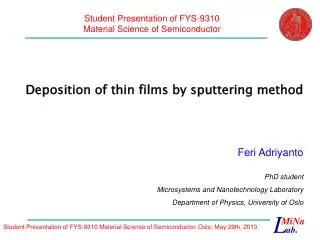
Student Presentation of FYS-9310 Material Science of Semiconductor. Deposition of thin films by sputtering method. Feri Adriyanto. PhD student Microsystems and Nanotechnology Laboratory Department of Physics, University of Oslo. Outline. Introduction. Fundamental of sputtering.

E N D
Student Presentation of FYS-9310 Material Science of Semiconductor Deposition of thin films by sputtering method Feri Adriyanto PhD student Microsystems and Nanotechnology Laboratory Department of Physics, University of Oslo
Outline • Introduction • Fundamental of sputtering • Techniques of sputtering • Sputtering zinc oxide thin film • Summary
Outline • Introduction • Fundamental of sputtering • Techniques of sputtering • Sputtering zinc oxide thin film • Summary
Mechanism of sputtering ? Interactions of ions with surfaces The ion impact may set up a series of collisions between atoms of the target, possibly leading to the ejection of some of these atoms. This ejection process is known as sputtering. The removal of surface atoms due to energetic particle bombardment http://www.postech.ac.kr/mse/tfxs/2003_2/chapter3.pdf
Sputter yield deposition Sputtering Ions are accelerated into target Some of the surface atoms are sputtered off of the target. These sputtered atoms “flow” across the chamber to where they are deposited Measure of efficiency of sputtering The sputter yield depends on: (a) the energy of the incident ions; (b) the masses of the ions and target atoms; (c) the binding energy of atoms in the solid and (d) the incident angle of ions.
Sputtering Alloy Targets • Slow diffusion mixing in solids (sputtering) • target reaches steady state • surface composition balances sputter yield Suiqiong Li, student presentation of ELEC 7730
Advantages & Disadvantagesof sputter deposition Disadvantages Advantages • Sputtering rates are low compared to those that can be attained in thermal evaporation. • Sputtering targets are often expensive and material use may be poor. • Most of the energy incident on the target becomes heat, which must be removed. • In reactive sputter deposition, the gas composition must be carefully controlled to prevent positioning the sputtering target. • Elements, alloys and compounds can be sputtered and deposited. • The sputtering target provides a stable, long-lived vaporization source. • In some configurations, reactive deposition can be easily accomplished using reactive gaseous species that are activated in plasma. • The source and substrate can be spaced close together. • The sputter deposition chamber can have a small volume.
Outline • Introduction • Fundamental of sputtering • Techniques of sputtering • Sputtering zinc oxide thin film • Summary
DC (diode) Sputtering The simplest sputtering technology Parameters for DC Sputtering • Sputter voltage • typically -2 to -5 kV • Substrate Bias Voltage • substrate is being bombarded by electrons and ions from target and plasma sputtering film while you deposit • neutral atoms deposit independently • put negative bias on the substrate to control this can significantly change film properties • Deposition rate • changes with Ar pressure • increases with sputter yield • usually increases with high voltage http://www.glue.umd.edu/~ddev/me489f/slides/2b_deposition_x6.pdf • E (e-) < 2eV - no ionization, elastic collisions only • E (e-) > 2eV - inelastic collisions add energy to Ar • ionization (highest energy process, ~15eV) • Note: mass (e-)/mass( Ar) ~ 10-5 • energy transfer small • e- gain energy via elastic collisions until E>15eV for ionization
Pressure ~10 Pa noble gas (e.g. Ar) Voltage ~1.5 kV • Disadvantages: • Low ion current density (low sputtering rate) Cathode 10 1 Ionisation coeffcient 0.1 - 0.01 • Electron emission • Sputtering • Implantation • Defects generation 10 100 + 1000 Electron energy [eV] • High working gas pressure resulting in scattering (low deposition rate) • Dielectric materials can not be sputtered • High voltage is needed Anode + substrate Fundamentals of plasma sputtering DC sputtering(diode sputtering) Tomasz Suszko, International Student Summer School„Nanotechnologies in materials engineering” Warsaw - Koszalin 2006
Low working gas pressure – 0.1 Pa • Very high ion current density is possible (high sputtering rate) 10 1 Ionisation coeffcient 0.1 0.01 10 100 1000 Electron energy [eV] Fundamentals of plasma sputtering (magnetron sputtering & unbalanced magnetron sputtering) G.J. Mankey, Lecture 9, Univ of Alabama There is a possibility to control the substrate ion current and the energy of the ions as well Substrate DC or pulsed power supply Tomasz Suszko, International Student Summer School„Nanotechnologies in materials engineering” Warsaw - Koszalin 2006
Advantages & Disadvantagesof Magnetron Sputtering Advantages • High deposition rate • Reducing electron bombardment of substrate • Extending the operating vacuum range • ability to operate at lower pressures The most widely commercially practiced sputtering method Disadvantages • An erosion track in the target • his leads to poor efficiency of sputtering yield versus target volume compared to non-magnetron sputtering • Non-uniform removal of particles from target result in non-uniform films on substrate
Reactive Sputtering Sputtering metallic target in the presence of a reactive gas mixed with inert gas (Ar) • A mixture of inert +reactive gases used for sputtering oxides – Al2O3, SiO2, Ta2O5 (O2) nitrides – TaN, TiN, Si3N4 (N2, NH3) carbides – TiC, WC, SiC (CH4, C2H4, C3H8) chemical reaction takes place on substrate and target can poison target if chemical reactions are faster than sputter rate adjust reactive gas flow to get good stoichiometry without incorporating excess gas into film
Gas pressure • Gas flows • Discharge power • (Substrate bias – energy of the ions) • (Substrate ion current density) Control unit Optical signal (optical emission spectroscopy) Fundamentals of plasma sputtering reactive sputtering Compounds of the target and gas elements Inert gas (e.g. Ar) Reactive gas (N2, O2, CH4 etc.) For poorly conducting or insulator deposits pulsed power supply is very usefull Pumping system
RF Sputtering • DC sputtering - what about dielectrics? • in DC systems, positive charge builds up on the cathode (target) need 1012 volts to sputter insulators !! avoid charge build up by alternating potential RF sputtering • frequencies less than about 50 kHz • electrons and ions in plasma are mobile • both follow the switching of the anode and cathode • basically DC sputtering of both surfaces • frequencies above about 50 kHz • ions (heavy) can no longer follow the switching • enough electrons to ionize gases(5~30MHz) • Typically 13.56 MHz is used
Advantages of RF Sputtering • It works well with insulating targets • High efficiency • easier to keep plasma going → can operate at lower Ar pressures (1-15 mTorr) → fewer gas collisions → more line of sight deposition http://aultimut.com/aultimut/details.asp?itemid=11
Outline • Introduction • Fundamental of sputtering • Techniques of sputtering • Sputtering zinc oxide thin film • Summary
Al-doped ZnO thin films for TCO applications Sample Prepared: The ZnO thin films were deposited onto glass and n-Si (100) substrate with Tri-Axis Semicore r.f. sputtering machine using 5% Al-doped ZnO target. Experimental conditions: Substrate temperature: 4000 C. Ar flow-rate: 30 sccm, 50 sccm, 60 sccm, 70 sccm and 80 sccm. r.f. power: 50 W and 200 W. Characterizations of sputtered sample: Thickness of the sputtered films: spectroscopic ellipsometry and dektak profilometry. Transmittance: UV-VIS-NIR spectroscopy. Crystal orientation: X-rays diffractometer. Surface morphology : AFM Resistivity: Hall measurement. Mobility : Hall measurement. chamber monitor target substrate Tri-Axis Semicore r.f. sputtering
X-rays diffraction spectra of sputtered Al-doped ZnO thin films AFM Dimension 3100 at SMN UiO • A strong X-ray peak from (002) and (004) planes is dominant, suggesting that most grains have c-axis perpendicular to the substrate surface. • The (002)-ZnOand (004)-ZnO peaks were measured at 2 = 34.120,and 71.850 Bruker AXS D8 Discover
Effect of sputtering power on the growth rate and transmittance at 480 nm • Growth rate of the Al-doped ZnO thin films increases nearly linearly from 1.0 to 5.4 nm/min when the sputtering power increases from 50 to 200 W • As the sputtering power increases from 50 to 150 W, the transmittance at 480 nm increases firstly from 83% to 92% and then decreases to 80%. The maximum transmittance of 92% was obtained at the sputtering power of 150 W. Rudolf Research / AutoEL Shimadzu SolidSpe-3700 DUV
Ar flow rate effect on the electrical properties of Al doped ZnO film Lakeshore 7704A Hall measurement http://www.caeonline.com/listing/product/183090/lakeshore-7704a • The resistivity of the films is decreases as the Ar flow rate is increased. The lowest resistivity of 9.74 x 10-4.cm was obtained at the films with Ar flow rate of 80 sccm. • The mobility increases with the Ar flow rate increases. • The carrier concentration also indicates the same pattern as the mobility
Outline • Introduction • Fundamental of sputtering • Techniques of sputtering • Sputtering zinc oxide thin film • Summary
Summary • Sputter deposition, also known as physical vapor deposition is a widely used technique for depositing thin films on semiconductor wafers. • The range of applications of sputtering and the variations of the basic process, is extremely wide. • ZnO thin films have been successfully deposited by rf sputtering and a promising transparent conductive oxide for application in thin film solar cells.